Photo mask and method for fabricating the same

a technology of photo mask and fabricated parts, applied in the field of photo mask, can solve the problems of poor aspect ratio, deterioration of the quality of the completed semiconductor device, and the inability of the isolating pattern hole hb>2/b> to have a normal shape, etc., and achieve the effect of increasing the production cost and improving the yield of the produ

Inactive Publication Date: 2005-06-30
DONGBU ELECTRONICS CO LTD
View PDF6 Cites 1 Cited by
  • Summary
  • Abstract
  • Description
  • Claims
  • Application Information

AI Technical Summary

Benefits of technology

[0012] An object of the present invention is to provide a photo mask and a method for fabricating the same in which a transparent substrate is covered with a phase inversion light-transmitting layer, a plurality of small sized light-transmitting holes are aggregately formed at dense intervals in an isolated pattern hole region of the phase inversion light-transmitting layer, and light transmited through the light-transmitting holes and the phase inversion light transmitted through the transmitting layer are guided to cause a series of interference phenomena such as sidelobe phenomena, so that the isolated pattern hole can sufficiently receive lights as the light intensity increases by way of the sidelobe phenomena.
[0013] Another object of the present invention is to provide a photo mask and a method for fabricating the same in which sidelobe phenomena regarded as a defect factor are used to allow an isolated pattern hole to sufficiently receive lights after aggregately forming small sized light-transmitting holes in an isolated pattern hole region of a transparent substrate, so that the step of additionally forming serif holes is naturally skipped, thereby improving yield of the product and controlling increase of the production cost.
[0017] The present inventor recognized that if the light energy from sidelobes, which is conventionally thought to be an unwanted effect, can be properly combined with sidelobes from light passing though adjacent holes, the desirable effect of providing high intensity at predetermined locations on the imaging area can be achieved by adding sidelobe energy that is in phase (or constructive adds).

Problems solved by technology

Thus, the isolated pattern hole H2 cannot have a normal shape (e.g., poor aspect ratio) when a series of process steps are finished.
Finally, the completed semiconductor device has deteriorated quality.
Moreover, since complicated process steps are required to additionally form the serif holes 7a, yield of the product may greatly be reduced and the production cost may increase rapidly.

Method used


Image

  • Photo mask and method for fabricating the same
  • Photo mask and method for fabricating the same
  • Photo mask and method for fabricating the same

Examples


Embodiment Construction

[0029] Reference will now be made in detail to the preferred embodiments of the present invention, examples of which are illustrated in the accompanying drawings. Wherever possible, the same reference numbers will be used throughout the drawings to refer to the same or like parts.

[0030] Hereinafter, a photo mask and a method for fabricating the same according to the present invention will be described as follows.

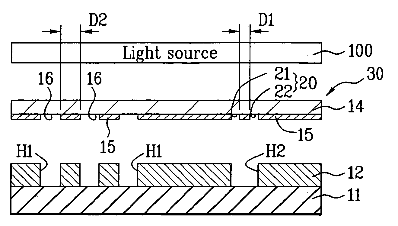
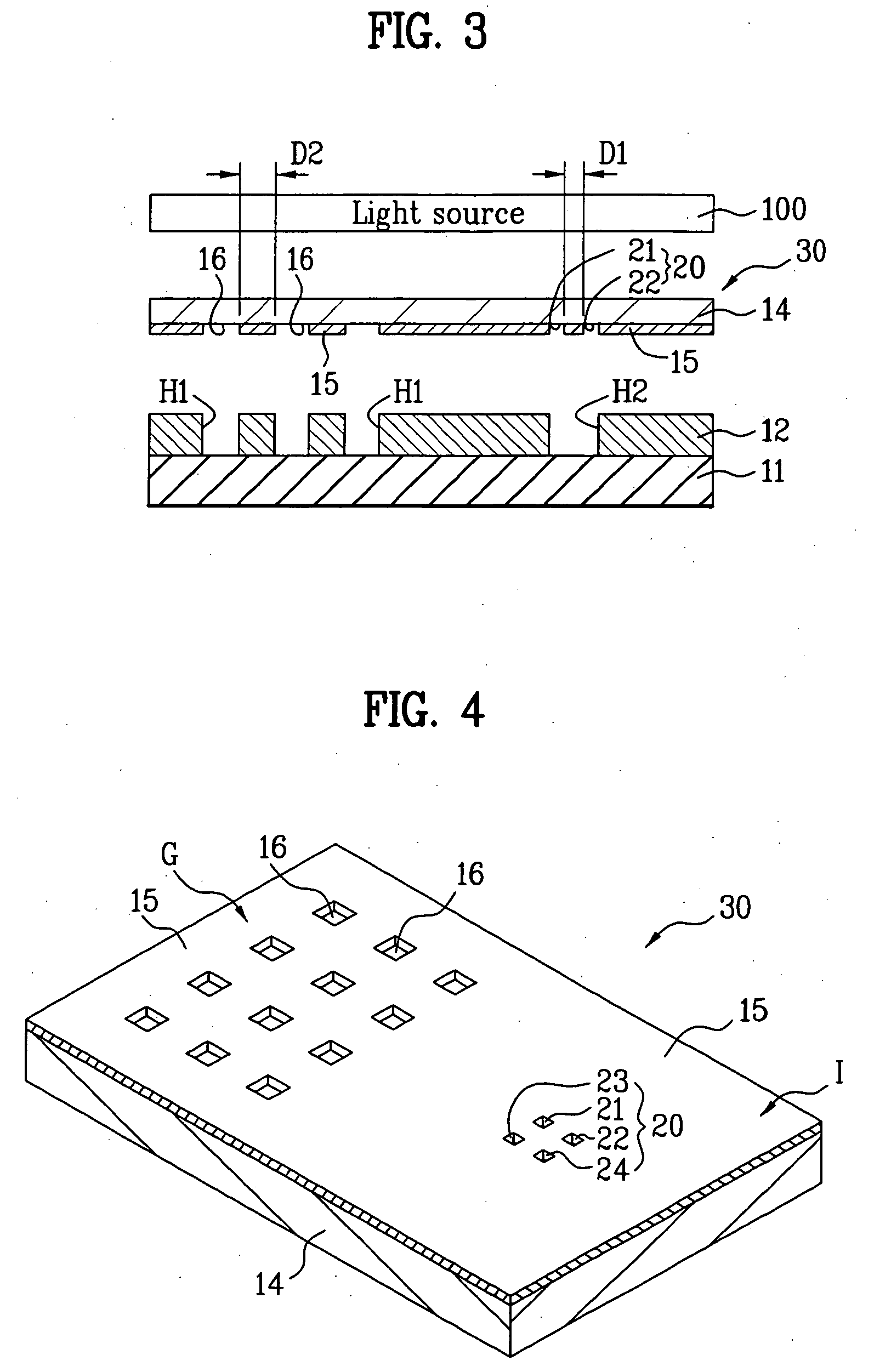
[0031] As shown in FIG. 3 and FIG. 4, a photo mask 30 of the present invention includes a transparent substrate 14, a phase inversion light-transmitting layer 15 covering the entire surface of the transparent substrate 14, and a plurality of light-transmitting holes 16 and 20 formed by opening the phase inversion light-transmitting layer 15. In this case, a glass substrate or a quartz substrate may optionally be used as the transparent substrate 14. Preferably, an attenuated type phase inversion light-transmitting layer may be used as the phase light-transmitting layer 15....


PUM

PropertyMeasurementUnit
sizeaaaaaaaaaa
transparentaaaaaaaaaa
phase inversionaaaaaaaaaa

Abstract

A photo mask and a method for fabricating the same are described, in which a transparent substrate is covered with a phase inversion light-transmitting layer, a plurality of small sized light-transmitting holes are aggregately formed at dense intervals in an isolated pattern hole region of the phase inversion light-transmitting layer, and lights transmitting the light-transmitting holes and the phase inversion light-transmitting layer are guided to cause a series of interference phenomena such as sidelobe phenomena, so that the isolated pattern hole can sufficiently receive lights as the light intensity increases by way of the sidelobe phenomena. If the sidelobe phenomena regarded as a defect factor are used to allow the isolated pattern hole to sufficiently receive lights after aggregately forming the small sized light-transmitting holes in the isolated pattern hole region of the transparent substrate, the step of additionally forming serif holes is naturally skipped, thereby improving yield of the product and controlling increase of the production cost.

Description

BACKGROUND OF THE INVENTION [0001] 1. Field of the Invention [0002] The present invention relates to a photo mask for use in fabricating a semiconductor device, and more particularly, to a photo mask and a method for fabricating the same in which a transparent substrate is covered with a phase inversion light-transmitting layer, a plurality of small sized light-transmitting holes are aggregately formed at dense intervals in an isolated pattern hole region of the phase inversion light-transmitting layer. Light that is transmited through the light-transmitting holes and phase inversion light are guided to cause a series of interference phenomena such as sidelobe phenomena, so that the isolated pattern hole can sufficiently receive sufficient light intensity in all portions thereof, including a center portion, (by way of the sidelobe phenomena) to create a via hole with excellent height to depth aspect ratio. [0003] 2. Discussion of the Related Art [0004] Recently, as semiconductor dev...

Claims


Application Information

Patent Timeline
Patent Type & Authority Applications(United States)
IPC IPC(8): G03C5/00G03F1/32G03F1/68G03F9/00H01L21/027
CPCG03F1/32H01L21/027
Inventor LEE, JUN SEOK
Owner DONGBU ELECTRONICS CO LTD
Why Eureka
Try Eureka