Fabrication method of self-aligned ferroelectric gate transistor using buffer layer of high etching selectivity
- Summary
- Abstract
- Description
- Claims
- Application Information
AI Technical Summary
Benefits of technology
Problems solved by technology
Method used
Image

Examples
Embodiment Construction
[0024] The present invention will now be described in detail.
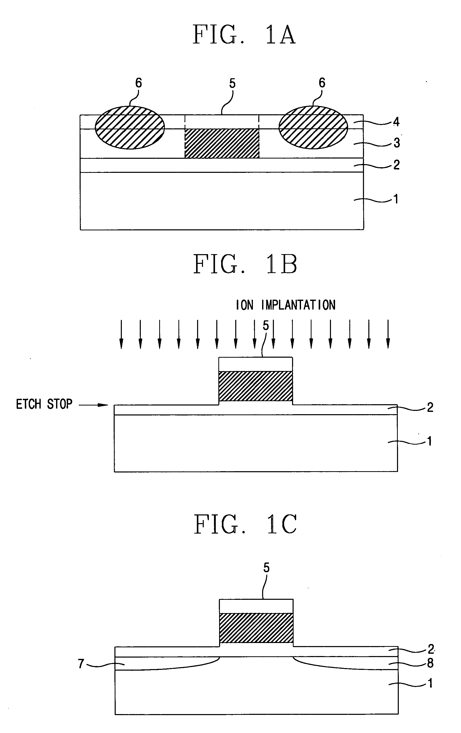
[0025]FIGS. 1A to 1C are sequential sectional views showing process of fabricating a self-aligned ferroelectric gate transistor in accordance with the present invention.
[0026] First, a buffer layer 2 made of a material with high etching selectivity is formed on a silicon substrate 1. The buffer layer 2 allows silicon at the portion where the source and drain will be formed not to be damaged when an upper electrode 4 and a ferroelectric layer 3 are etched. In the present invention, as a material with a high etching selectivity, CeO2 or Y2O3 may be used.
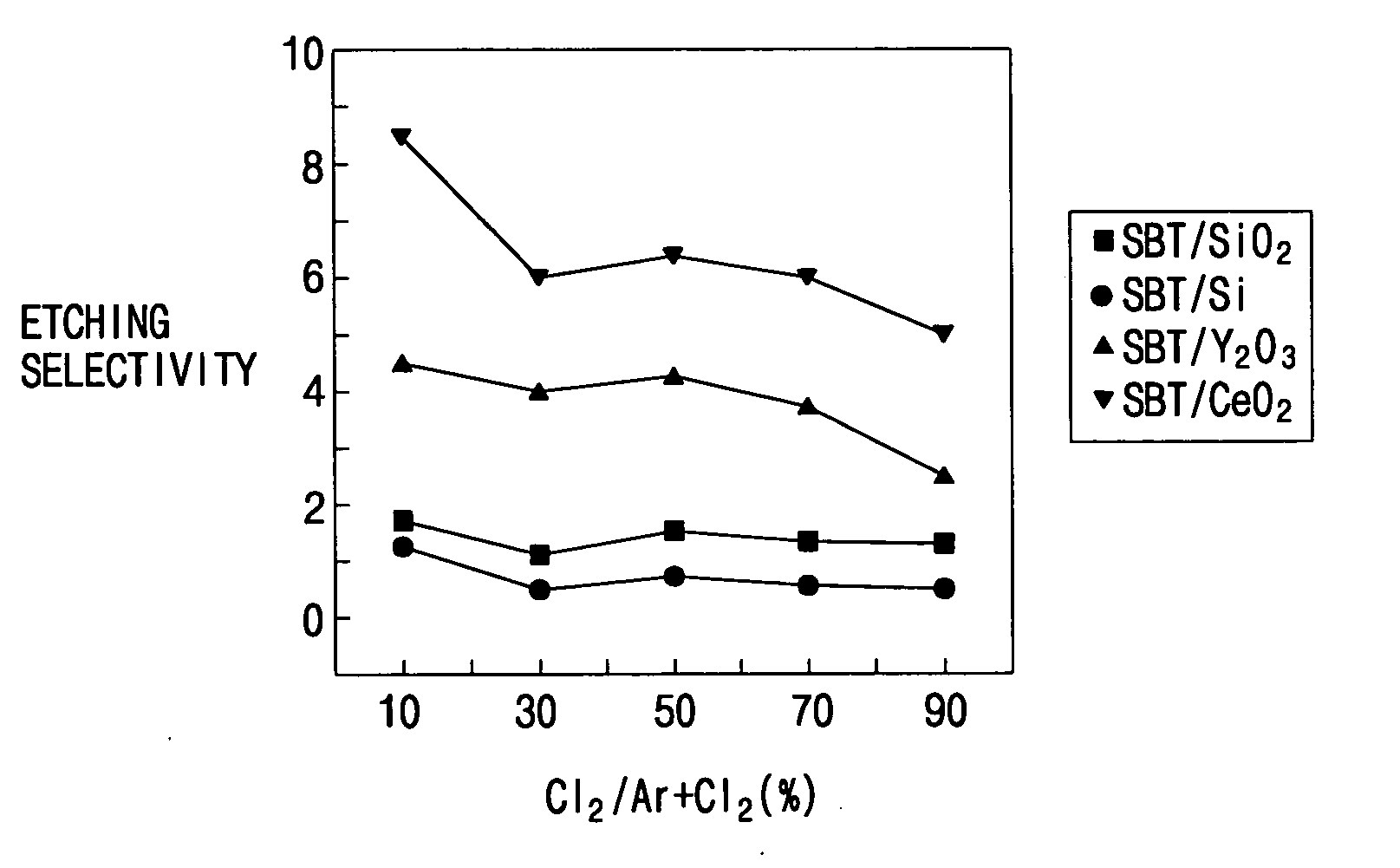
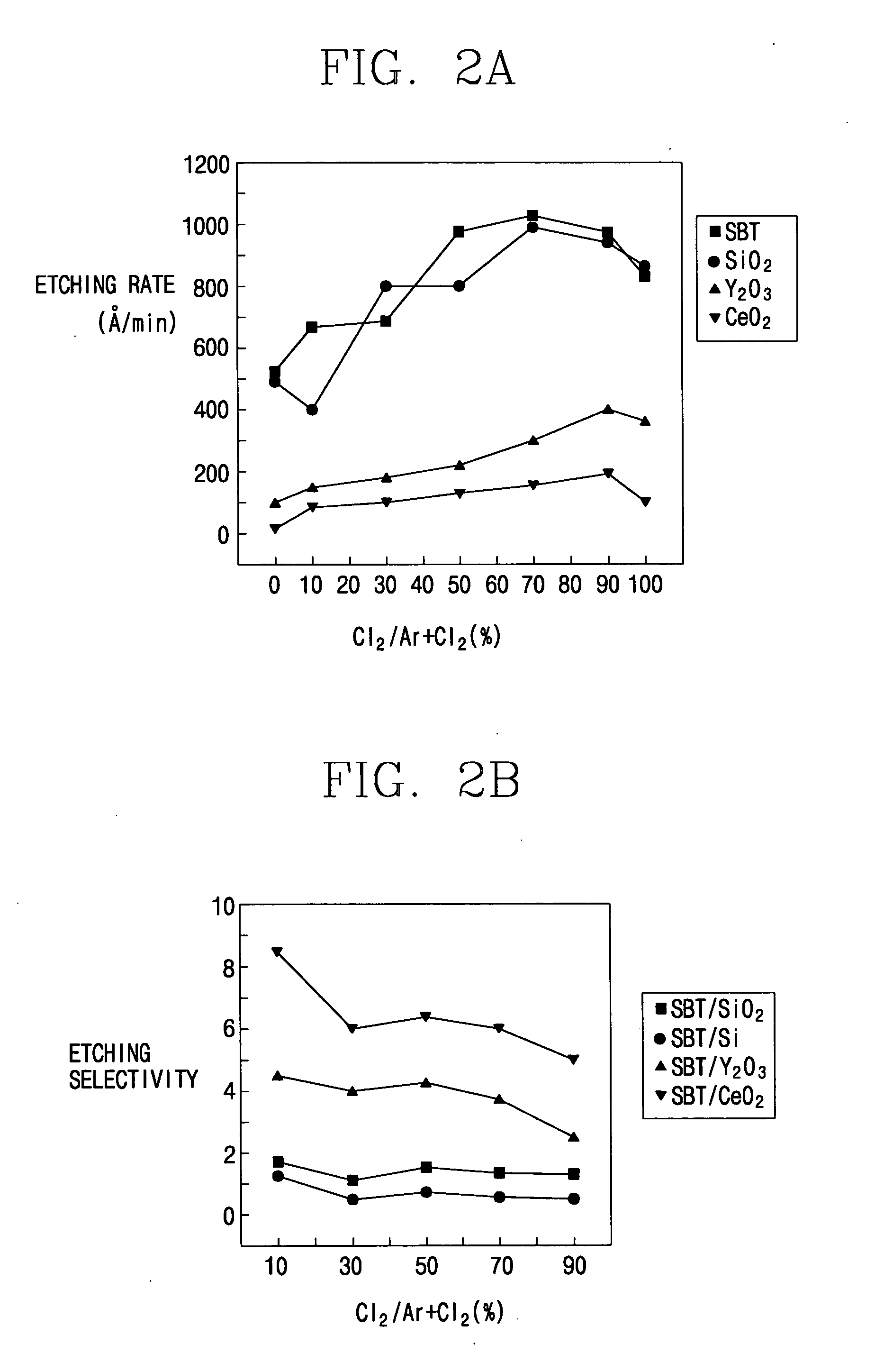
[0027]FIG. 2A is a graph showing etching rates of SBT, SiO2 and materials (CeO2 or Y2O3) used as the buffer layer in a dry etching using Cl2 / Ar+Cl2 gas. In FIG. 2A, it is noted that as the amount of Cl2 increases, the etching rates of SBT thin film and SiO2 thin film remarkably increase whereas etching rates of CeO2 or Y2O3 increase very small.
[0028]FIG. 2B shows etching ...
PUM
 Abstract
Description
Claims
Application Information
 - R&D
- Intellectual Property
- Life Sciences
- Materials
- Tech Scout
- Unparalleled Data Quality
- Higher Quality Content
- 60% Fewer Hallucinations
Browse by: Latest US Patents, China's latest patents, Technical Efficacy Thesaurus, Application Domain, Technology Topic, Popular Technical Reports.
© 2025 PatSnap. All rights reserved.Legal|Privacy policy|Modern Slavery Act Transparency Statement|Sitemap|About US| Contact US: help@patsnap.com