Method of processing selected surfaces in a semiconductor process chamber based on a temperature differential between surfaces

a technology of semiconductor process chamber and temperature differential, which is applied in the direction of cleaning using liquids, instruments, optical radiation measurement, etc., can solve the problems of rtp system certain disadvantages that have not been adequately addressed, defective devices being formed on the wafer, and prolonged heating and cooling of the wafer

Inactive Publication Date: 2005-07-14
MICRON TECH INC
View PDF5 Cites 1 Cited by
  • Summary
  • Abstract
  • Description
  • Claims
  • Application Information

AI Technical Summary

Benefits of technology

[0013] The present invention overcomes the disadvantages of the prior art by providing a method by which a reactant may favor a reaction with selected surfaces in a semiconductor process chamber. In so doing, the present invention overcomes the problem of using a reactant that would act desirably on some surfaces and detrimentally on other surfaces.
[0014] The present invention provides a method that will facilitate the cleaning of RTP process chambers, thereby better facilitating the adoption and use of RTP systems. More particularly, the present invention overcomes the inherent disadvantages of using a powerful etchant, such as NF3 gas to clean an RTP process chamber.
[0015] The present invention also overcomes the problems of high particle counts and lowered production yields that result if NF3 gas or other strong etchant is used to clean RTP process chambers. Accordingly, the present invention also improves the process of HSG formation in RTP process chambers.

Problems solved by technology

Unnecessary heating may lead to defective devices being formed on the wafer.
Thus, in hot wall process chambers a wafer may be subject to prolonged heating and cooling.
However, RTP systems have certain disadvantages that have not been adequately addressed.
One significant disadvantage is that radiant energy may not be absorbed uniformly by a wafer.
This results in temperature variations in and across the wafer.
Temperature variations lead to non-uniform process results.
Unfortunately, a significant disadvantage of this temperature monitoring system is its vulnerability to certain cleaning processes carried out in an RTP process chamber.
Poor, irregular HSG formations result in unclean RTCVD process chambers.
An undesired side effect from polysilicon deposition is that the polysilicon is deposited not only on the wafer but also on other surfaces in the process chamber.
A build-up of polysilicon impedes the transmission of radiant energy through the window onto the wafer.
It may also lead to high particle counts in the chamber, lowering production yields.
The '195 patent does not teach or suggest that the described cleaning system is suitable for use in “cold wall”, RTP systems, including RTCVD systems.
However, NF3's high reactivity has so far limited its usefulness in this regard.
NF3 cleaning, until the present invention, has not proved suitable for use in cold wall systems, such as RTCVD systems, because certain components in RTCVD chambers may be damaged by the high activity of NF3 at higher temperatures.
The temperatures that occur in RTCVD processing can exceed 750° C. At such temperatures, NF3 is so corrosive that it attacks stainless steel, quartz, and silicon surfaces, damaging critical components found in RTCVD process chambers.
As mentioned, temperature-monitoring systems based on wafer emissivity are particularly vulnerable to damage.
NF3's action on such unintended targets may also create unacceptably high particle counts in the process chamber, lowering production yields.
If the NF3 cleaning is performed at lower temperatures, the etching rate is too low to effectively clean the system.
This results in unacceptably low etching rates.

Method used


Image

  • Method of processing selected surfaces in a semiconductor process chamber based on a temperature differential between surfaces
  • Method of processing selected surfaces in a semiconductor process chamber based on a temperature differential between surfaces
  • Method of processing selected surfaces in a semiconductor process chamber based on a temperature differential between surfaces

Examples


Embodiment Construction

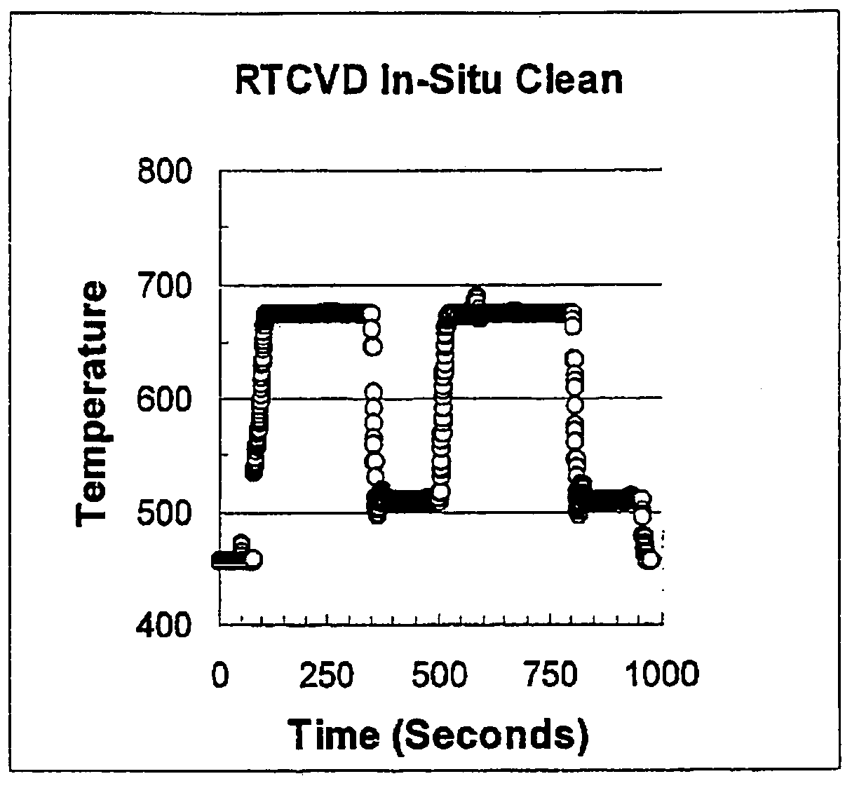
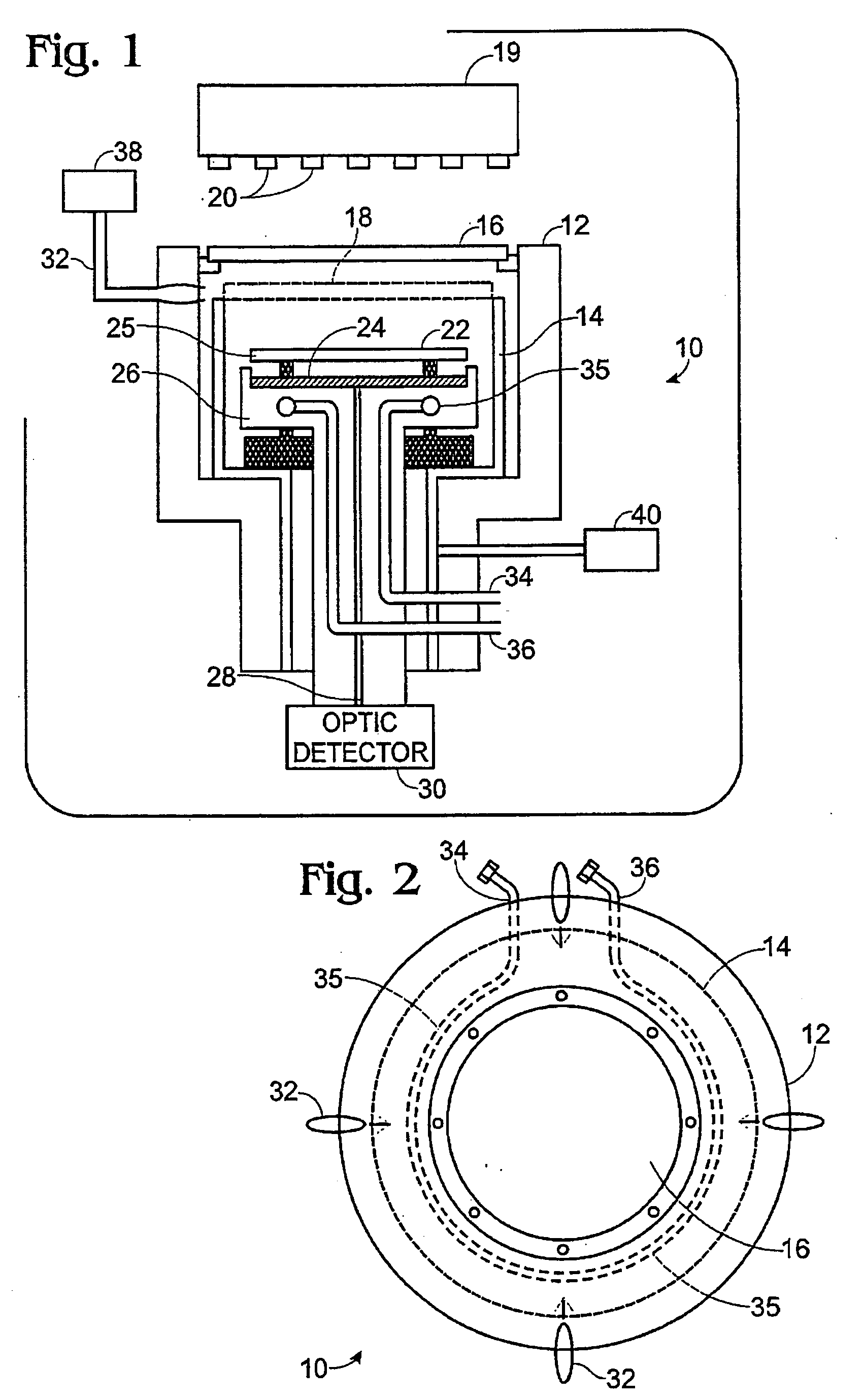
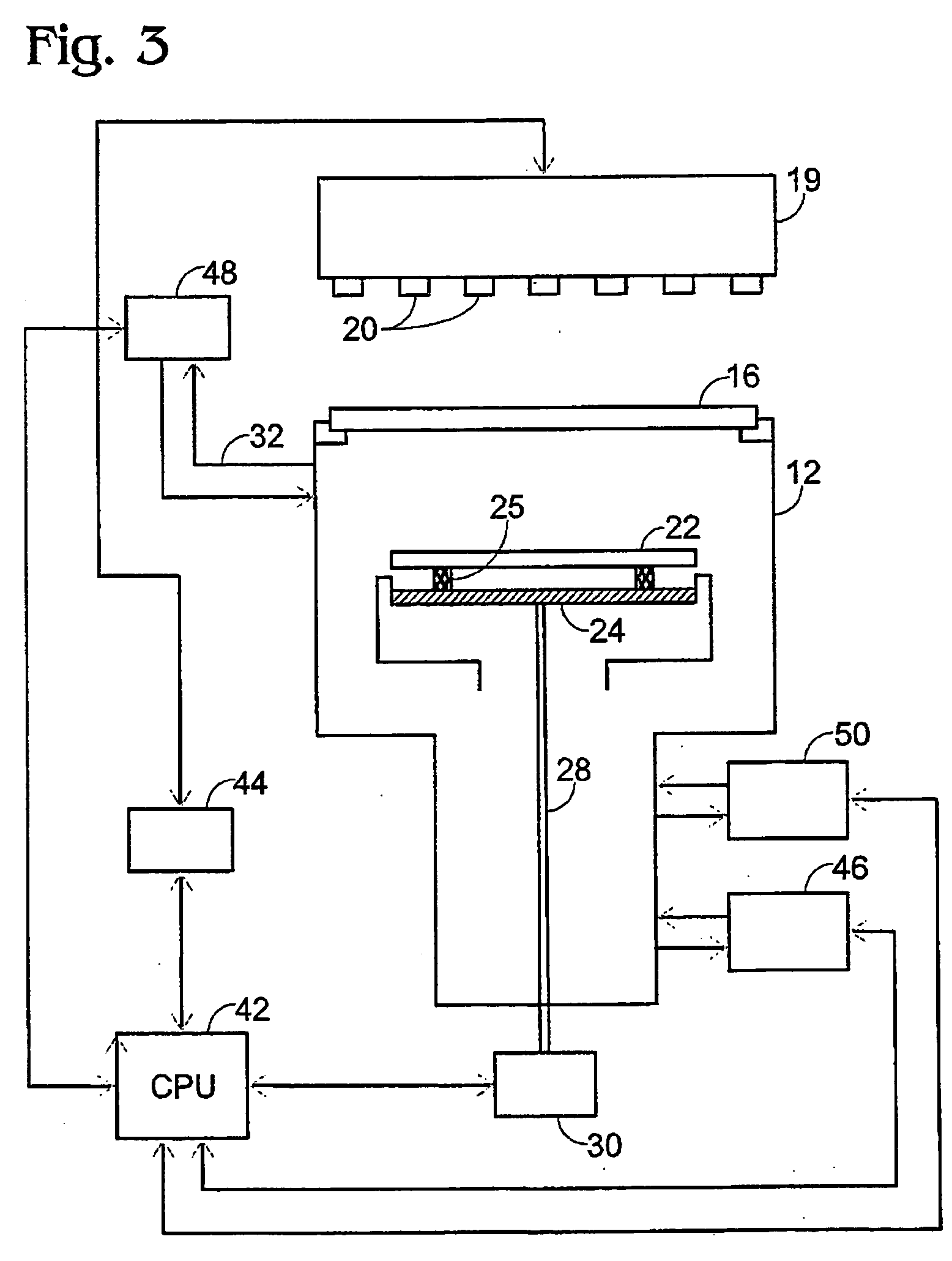
[0036] In this invention, a process chamber is a vessel where processes are being performed to fabricate discrete devices or circuits on a work object. The process chamber may be used to oxidize, etch, dope, deposit, implant or pattern materials in or on the work object, as well as to clean, prepare and condition the work object, among other things. The present invention is preferably used to process work objects in an RTP process chamber for chemical deposition, where the work object is heated to a higher temperature than surrounding walls in the chamber.

[0037]“Work object” means objects, including, wafers (including production, dummy, or pmon), die and packaged parts, incorporating, in whole or part, silicon substrates, and other known or discovered semiconductor materials, components, and assemblies, including, for example, silicon-on-insulator (SOI), silicon-on-sapphire (SOS), thin film transistor (TFT) materials, or germanium, periodic group III-IV materials, II-VI materials, ...


PUM

PropertyMeasurementUnit
temperatureaaaaaaaaaa

Abstract

The present invention relates to a method of processing selected surfaces in a semiconductor process chamber by creating a temperature differential between the selected surfaces and contacting the surfaces with a reactant that preferentially react with a surface at one end of the temperature differential relative to the other selected surface(s). More particularly, the invention relates to the use of nitrogen trifluoride (NF3) gas for in situ cleaning of cold wall process chambers such as Rapid thermal Chemical Vaporization (“RTCVD”) systems.

Description

BACKGROUND OF THE INVENTION [0001] The present invention relates to a method of processing a selected surface in a semiconductor process chamber by contacting the selected surface with a reactant that reacts preferentially with the selected surface relative to another surface when the selected surface is at a different temperature from the other surface. The invention is particularly suited for use in rapid thermal processing (RTP) systems. More particularly, the invention relates to the use of nitrogen trifluoride (“NF3”) gas to clean selected surfaces in RTP process chambers, including in Rapid Thermal Chemical Vapor Deposition (RTCVD) process chambers. [0002] During the course of semiconductor device fabrication, a wafer undergoes many steps of processing. Some steps involve heating the wafer hundreds of degrees Celsius above ambient temperature. Unnecessary heating may lead to defective devices being formed on the wafer. One reason for this is that heat causes substances, such a...

Claims


Application Information

Patent Timeline
Patent Type & Authority Applications(United States)
IPC IPC(8): C23C16/44
CPCY10S438/905C23C16/4405
Inventor PAN, JAMES
Owner MICRON TECH INC
Why Eureka
Try Eureka