Color filter substrate, liquid crystal display apparatus including color filter substrate, and method of manufacturing color filter substrate
- Summary
- Abstract
- Description
- Claims
- Application Information
AI Technical Summary
Benefits of technology
Problems solved by technology
Method used
Image
Examples
embodiment 1
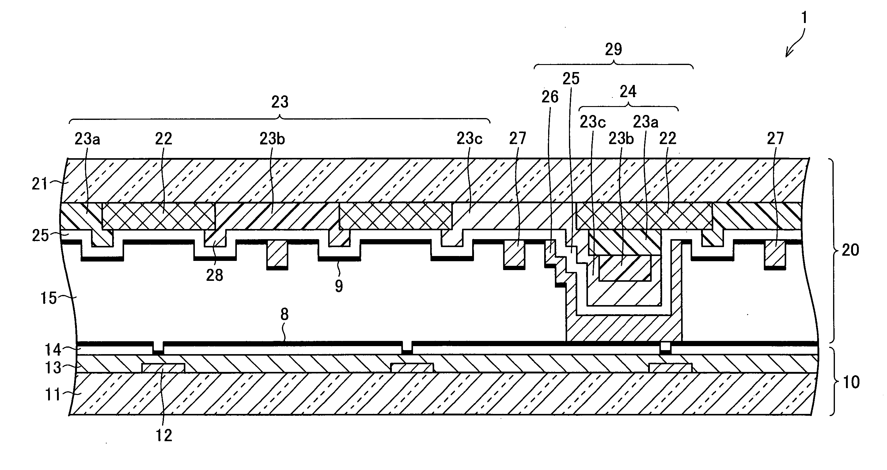
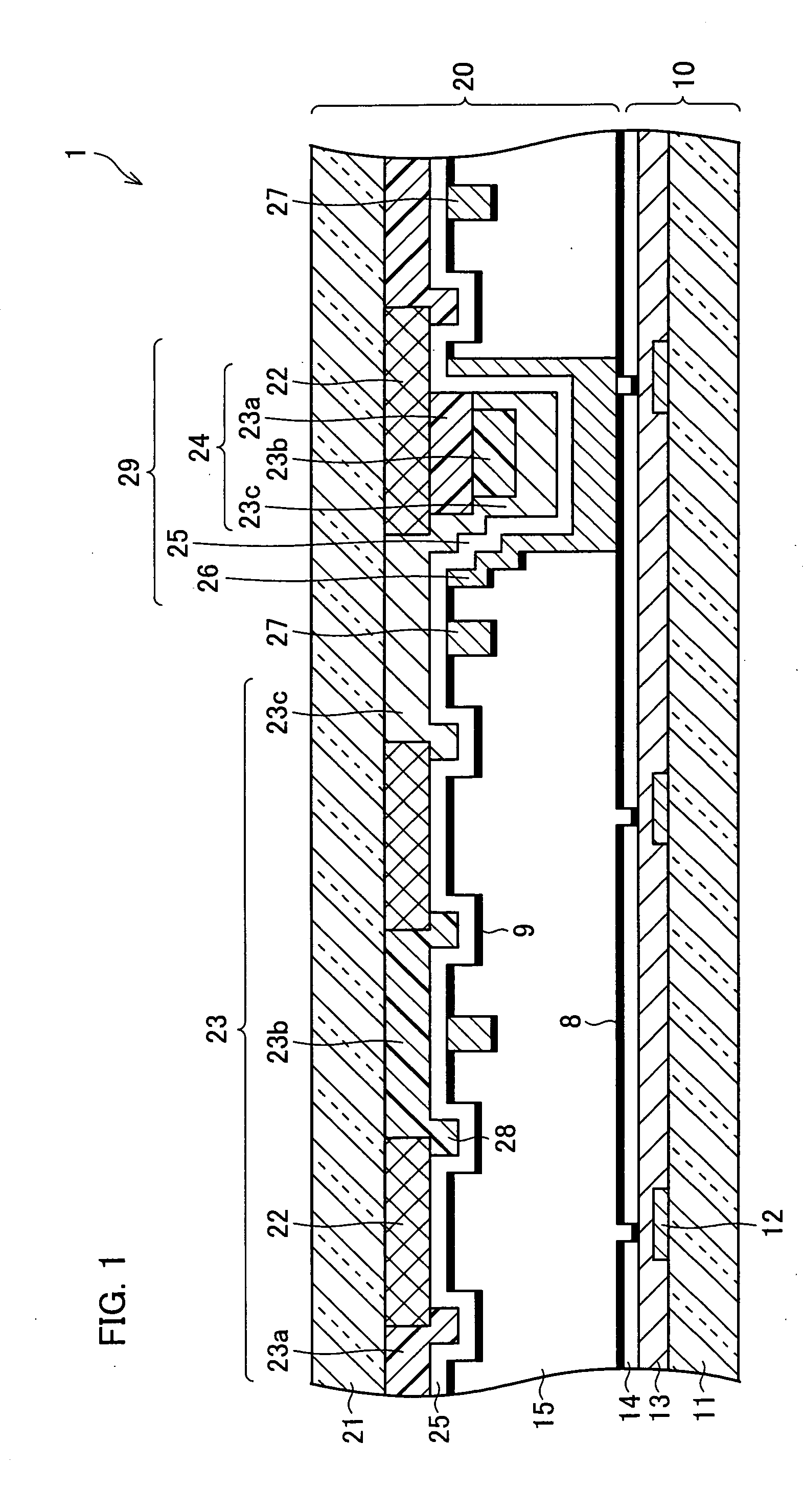
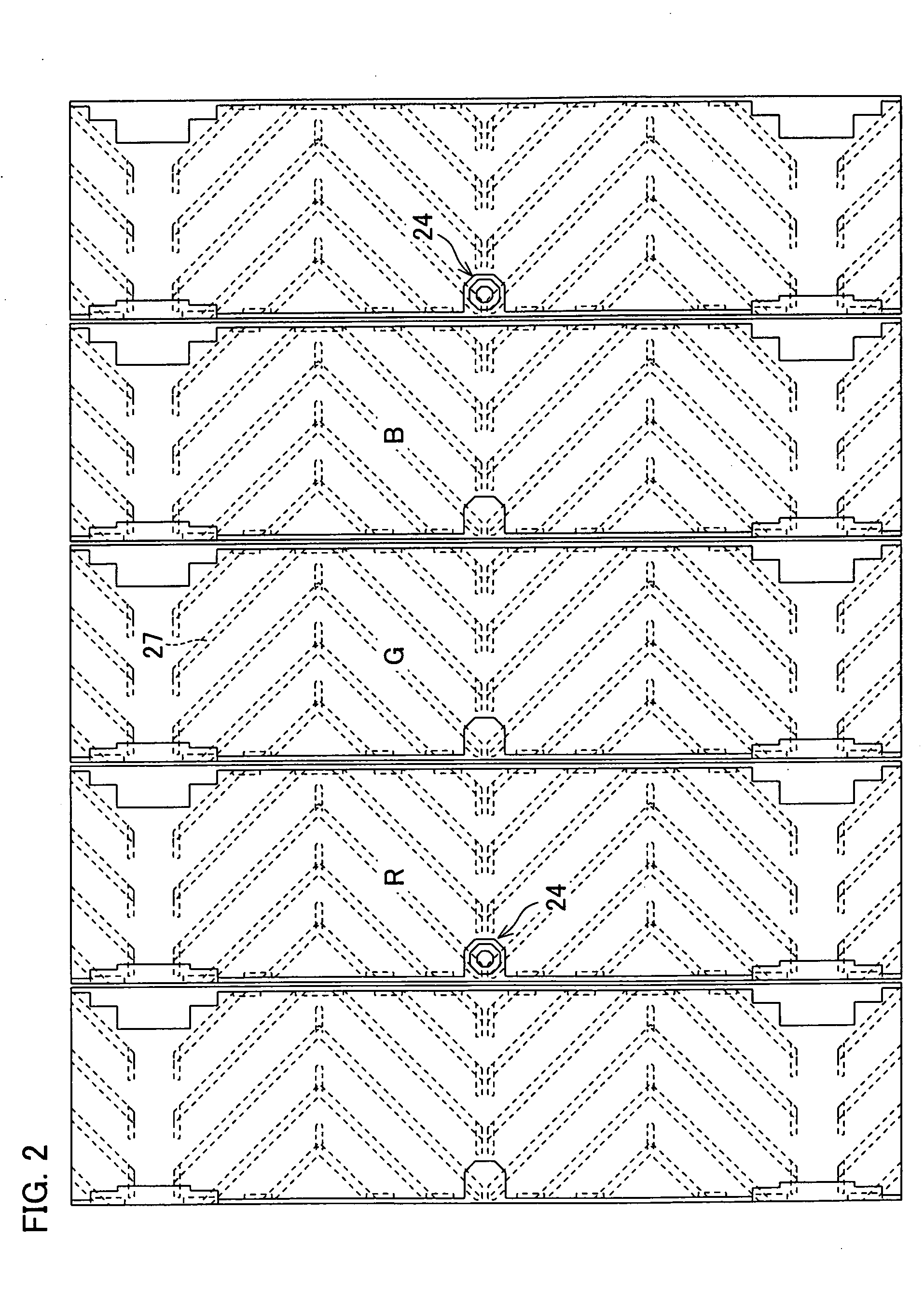
[0037] The following will describe an embodiment of the present invention in reference to FIGS. 1-6. FIG. 1 is a cross section of a liquid crystal display apparatus 1 of the present embodiment. FIG. 2 is a plan view of a color filter substrate of the present embodiment. Note that the liquid crystal display apparatus 1 of the present embodiment has a MVA (Multi-domain Vertical Alignment) structure. The structure of the liquid crystal display apparatus 1, however, is not limited to this MVA. Note that, the MVA structure is such an arrangement that liquid crystal molecules between a pair of substrate are vertically aligned when no voltage is applied, and one pixel is partitioned into more than one domain. That is, in the MVA structure, one pixel is partitioned into more than one domain in order to improve the viewing angle characteristics of a vertically-aligned liquid crystal display apparatus, and there are such methods of forming the domains as: cutting off, in a slit-shape, a pixel...
embodiment 2
[0071] Another embodiment of the present invention will be described in reference to FIGS. 7-9. By the way, members having the same functions as those described in Embodiment 1 with figures are given the same numbers, so that the descriptions are omitted for the sake of convenience.
[0072] Being similar to the liquid crystal display apparatus illustrated in Embodiment 1, a liquid crystal display apparatus of the present embodiment is arranged such that an insulative resin film is provided on a stacked layer of a color filter substrate, and the stacked layer and the insulative resin film function as a spacer so that a cell gap is formed. The cell gap is formed with the spacer being elastically deformed to an appropriate degree, by suitably setting the size of the contact region between the insulative resin film on the color filter substrate and a pixel electrode of a TFT array substrate.
[0073] When the contact region between the insulative resin film and the pixel electrode is too l...
embodiment 3
[0093] The following will discuss a further embodiment of the present invention in reference to FIGS. 10-12. By the way, members having the same functions as those described in Embodiment 1 with figures are given the same numbers, so that the descriptions are omitted for the sake of convenience.
[0094] In the stacked layer 24 as said at least one protruding structure section of Embodiments 1 and 2, not less than color layers (including the black matrix layer 22) are stacked. Present invention, however, is not limited to this, so that said at least one protruding structure section may include only two layers.
[0095]FIG. 10 shows a liquid crystal display apparatus 3 of the present embodiment. The liquid crystal display apparatus 3 does not include the black matrix layer 22 described in Embodiments 1 and 2, while includes a color filter substrate 40 that includes a stacked layer 44 in place of the stacked layer 24 and includes an insulative resin film (insulating layer) 46 in place of ...
PUM
 Abstract
Description
Claims
Application Information


