Planar lightwave circuit waveguide bends and beamsplitters

a waveguide and beam splitter technology, applied in the field of plane lightwave circuits, can solve the problems of limiting device size reduction, high refractive index contrast waveguides giving rise to more scattering loss than low refractive indexes, and limiting device scale integration

Inactive Publication Date: 2005-07-14
UNIVERSITY OF ALABAMA
View PDF15 Cites 8 Cited by
  • Summary
  • Abstract
  • Description
  • Claims
  • Application Information

AI Technical Summary

Benefits of technology

[0007] According to one embodiment of the invention, a planar lightwave circuit comprises a waveguide having a bend through which the waveguide direction is changed, in one embodiment as much as 90°. A plurality of trenches having parallel front and back interfaces are disposed on the bend. The trench has a refractive index different than the first refractive index so as to create a refractive interface between the waveguide and the trench. In some embodiments, the trench co...

Problems solved by technology

Low refractive index contrast waveguides in low index materials such as silica typically have a minimum bend radius of millimeters to several centimeters, which limits device size reduction.
However, for a given level of interface roughness between the core and clad materials, high refractive index contrast waveguides give rise to more scatt...

Method used


Image

  • Planar lightwave circuit waveguide bends and beamsplitters
  • Planar lightwave circuit waveguide bends and beamsplitters
  • Planar lightwave circuit waveguide bends and beamsplitters

Examples


Embodiment Construction

[0032] The inventions now will be described more fully hereinafter with reference to the accompanying drawings, in which some, but not all embodiments of the inventions are shown. Indeed, these inventions may be embodied in many different forms and should not be construed as limited to the embodiments set forth herein; rather, these embodiments are provided so that this disclosure will satisfy applicable legal requirements. Like numbers refer to like elements throughout.

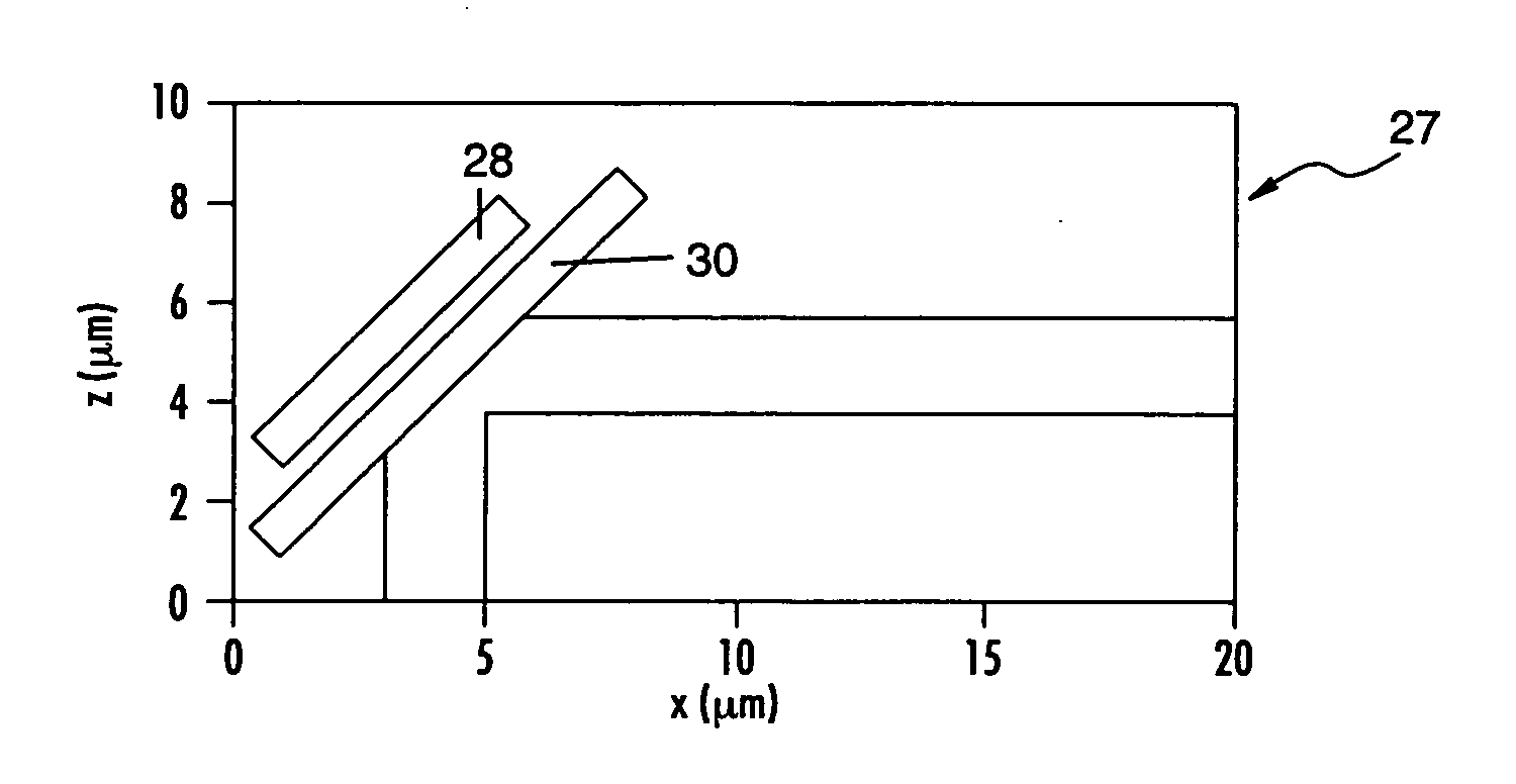
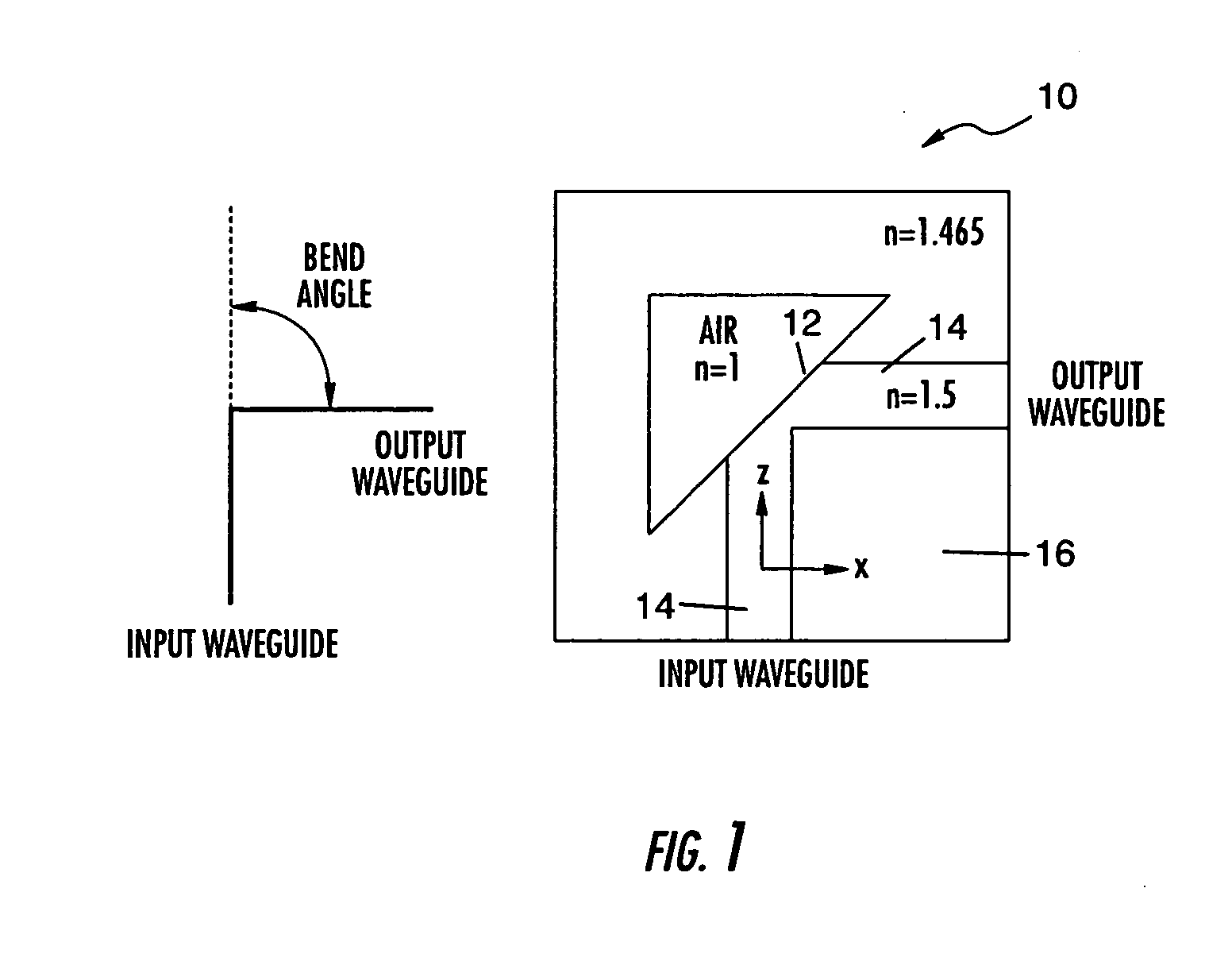
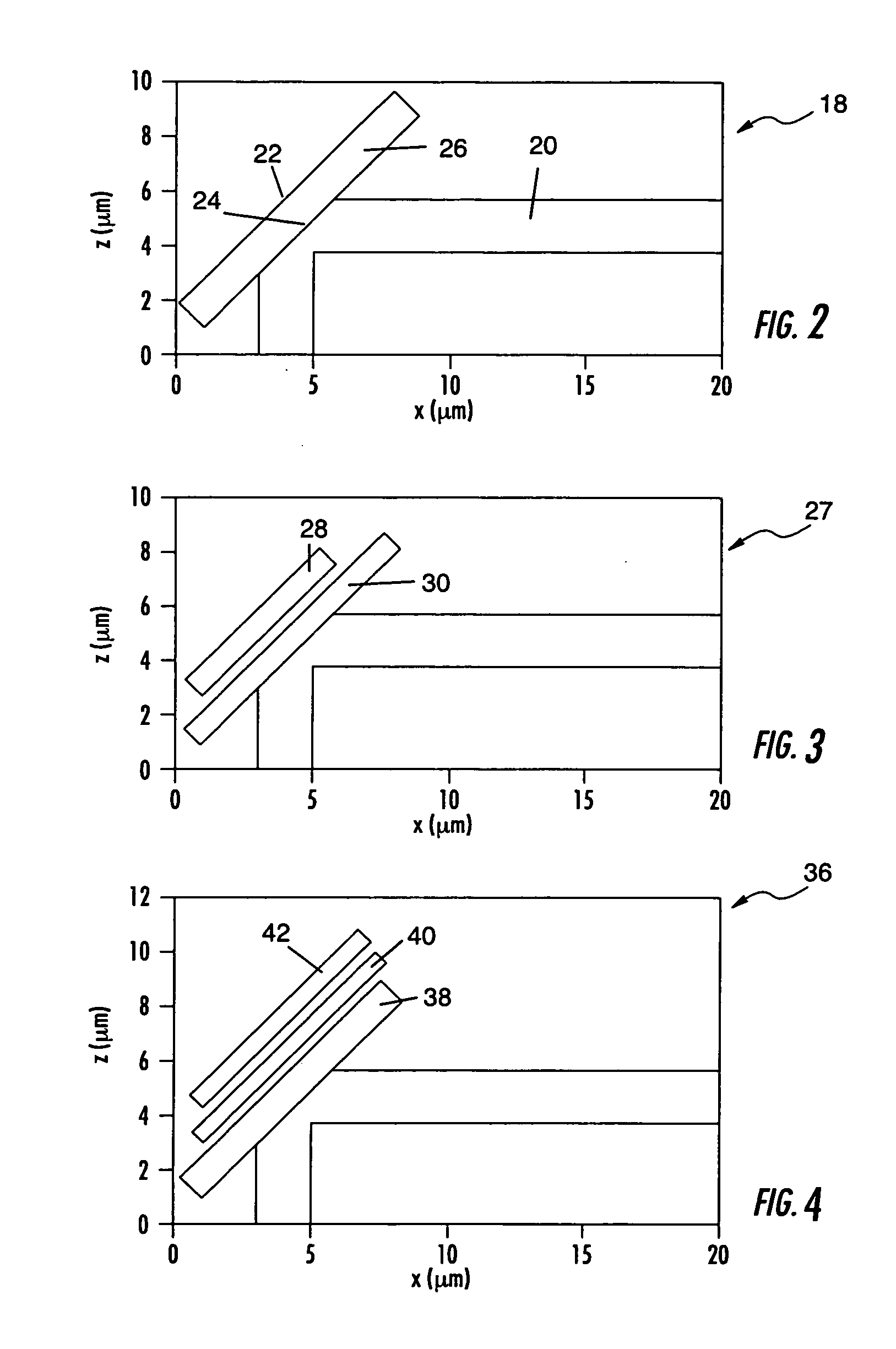
[0033] The apparatuses of the invention are based on multiple planar interfaces as a result of etched trenches. In this regard, embodiments are described in conjunction with etched air trenches in a planar lightwave circuit and etched air trenches that are filled with high refractive index silicon. Other embodiments will be recognized by one of ordinary skill in the art from the description herein, and such planar interfaces may be comprised of other materials having refractive indices and refractive index contrasts...


PUM


Abstract

A planar lightwave circuit has a waveguide having a bend and plurality of multiple trenches with parallel front and back interfaces. The trench and waveguide refractive indexes are different such that a refractive interface is defined between the waveguide and the trench. The trench may include a material of higher refractive index than the waveguide, such as silicon, or alternatively a material having a lower refractive index than the waveguide, such as an air void. The trench is disposed on the waveguide bend such that the front and back planar interfaces have an angle of incidence to a direction of the lightwave propagation from the waveguide. The invention also includes beamsplitters that include trenches that reflect a portion of a lightwave in a first direction and a portion of a lightwave in a second direction.

Description

CROSS-REFERENCE TO RELATED APPLICATIONS [0001] This application claims the benefit of the filing date of U.S. Provisional Patent Application Ser. No. 60 / 514,030 filed Oct. 24, 2003, which is hereby incorporated by reference.FEDERALLY SPONSORED RESEARCH OR DEVELOPMENT [0002] The research underlying this invention was supported in part with fuds from DARPA grant no. N66001-01-1-8938 and National Science Foundation grant EPS-0091853. The United States Government may have an interest in the subject matter of this invention.FIELD OF THE INVENTION [0003] The invention relates to planar lightwave circuits, and more particularly, to planar lightwave circuit waveguide bends and beamsplitters having multiple planar interfaces. BACKGROUND OF THE INVENTION [0004] Reducing the size of waveguide components enables higher levels of integration in planar lightwave circuits (PLCs). Waveguide bends and splitters heavily influence overall component size. Low refractive index contrast waveguides in low...

Claims


Application Information

Patent Timeline
IPC IPC(8): G02B6/126
CPCG02B6/126
Inventor LI, LIXIANORDIN, GREGORY P.JIANG, JIANHUAENGLISH, JENNIFER M.
Owner UNIVERSITY OF ALABAMA
Why Eureka
Try Eureka