Method of forming fet silicide gate structures incorporating inner spacers
- Summary
- Abstract
- Description
- Claims
- Application Information
AI Technical Summary
Problems solved by technology
Method used
Image
Examples
first embodiment
LAYER FOR INNER SPACER
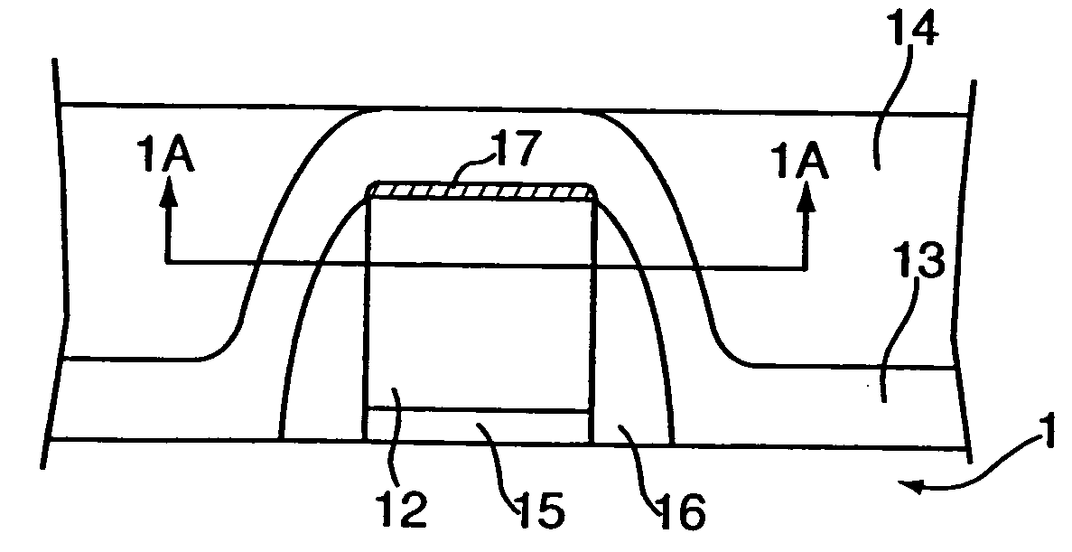
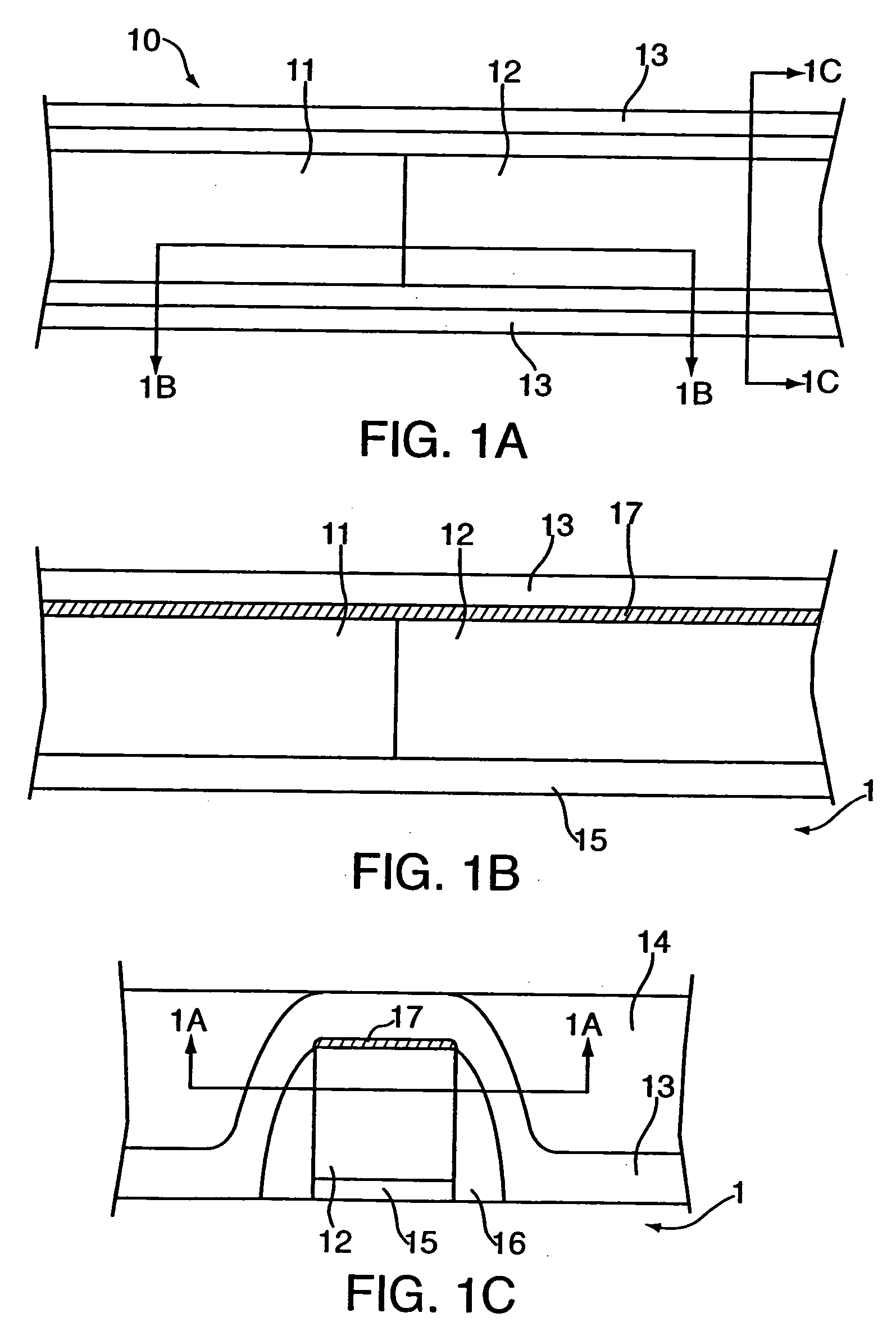
[0020] In this embodiment, an inner spacer, typically of silicon nitride, is formed in the trench created by removal of the polysilicon gate; this inner spacer permits separate formation of silicide gates in different regions. FIG. 3 is a transverse cross-section view of the structure at the beginning of the process, showing the nitride etch stop 13 and HDP oxide 14 overlying hardmask 17 and gate region 12, with nitride spacers 16 on either side of the polysilicon gate. As shown in FIG. 3, the structure has been planarized after the nitride and oxide deposition processes. The entire structure (both n+ and p+ regions) is further planarized to expose the hardmask 17 (see FIG. 4).
[0021] At this point the hardmask covering the n+ gate region 11 (not shown) is covered with photoresist 50, so that the only exposed hardmask is that covering region 12. The exposed hardmask 17 is removed, and then the underlying p+ polysilicon gate 12 and gate oxide 15 are also removed...
second embodiment
YER
[0028] In this embodiment, the blanket nitride layer 62 is etched so that only the sidewalls of the trench are covered by the inner spacer. The gate structure is processed as described in the first embodiment, to the point shown in FIG. 6 (that is, a blanket nitride layer 62 covers the sidewalls and bottom of the trench). Layer 62 is then etched using a directional process such as reactive ion etching (RIE). As a result of this process, nitride 62 and the thin gate oxide 61 are removed from the bottom of the trench, so that substrate 1 is again exposed; in addition, the edge of the nitride layer closest to the top of the trench is lowered and given a more rounded shape (see FIG. 10). A new gate dielectric 110 is formed at the bottom of the trench, and a blanket layer of polysilicon is deposited which fills the trench (FIG. 11). The polysilicon layer 112 is then planarized to again expose the hardmask 17 covering the other gate region and to again expose the HDP oxide 14 surroundi...
PUM
 Abstract
Description
Claims
Application Information
 - R&D Engineer
- R&D Manager
- IP Professional
- Industry Leading Data Capabilities
- Powerful AI technology
- Patent DNA Extraction
Browse by: Latest US Patents, China's latest patents, Technical Efficacy Thesaurus, Application Domain, Technology Topic, Popular Technical Reports.
© 2024 PatSnap. All rights reserved.Legal|Privacy policy|Modern Slavery Act Transparency Statement|Sitemap|About US| Contact US: help@patsnap.com


