Semiconductor integrated circuit device
- Summary
- Abstract
- Description
- Claims
- Application Information
AI Technical Summary
Benefits of technology
Problems solved by technology
Method used
Image
Examples
first embodiment
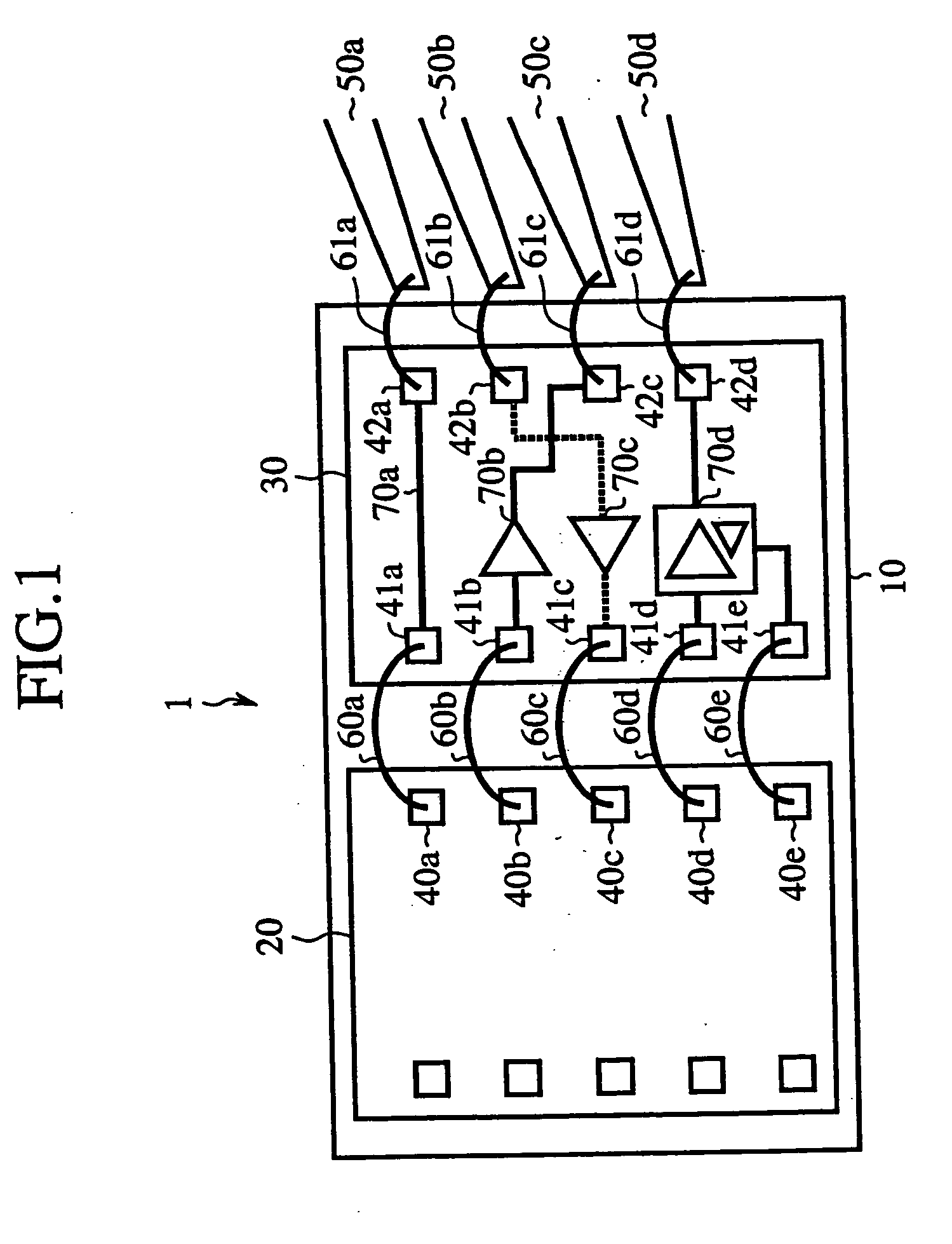
[0049]FIG. 1 is a plan view showing a semiconductor integrated circuit device according to a first embodiment of the present invention. In FIG. 1, reference numeral 1 indicates a semiconductor integrated circuit device. Reference numeral 10 indicates a bonding pad (bonding PAD), reference numeral 20 indicates a semiconductor integrated circuit chip A (Chip. A) disposed on the bonding PAD 10, and reference numeral 30 indicates a semiconductor integrated circuit chip B (Chip B) including interface functions (I / F functions), which is disposed on the bonding PAD 10, respectively. Reference numerals 40a-40e indicate pads (PADs) of the Chip A20, and reference numerals 41a-41e and 42a-42d indicate pads (PADs) of the Chip B30, respectively. Reference numerals 50a-50d indicate leads (LEADs) disposed around arrays of the Chip A20 and Chip B30 disposed on the bonding PAD 10. Reference numerals 60a-60e and 61a-61d respectively indicate bonding wires. Reference numeral 70a indicates a wiring ele...
second embodiment
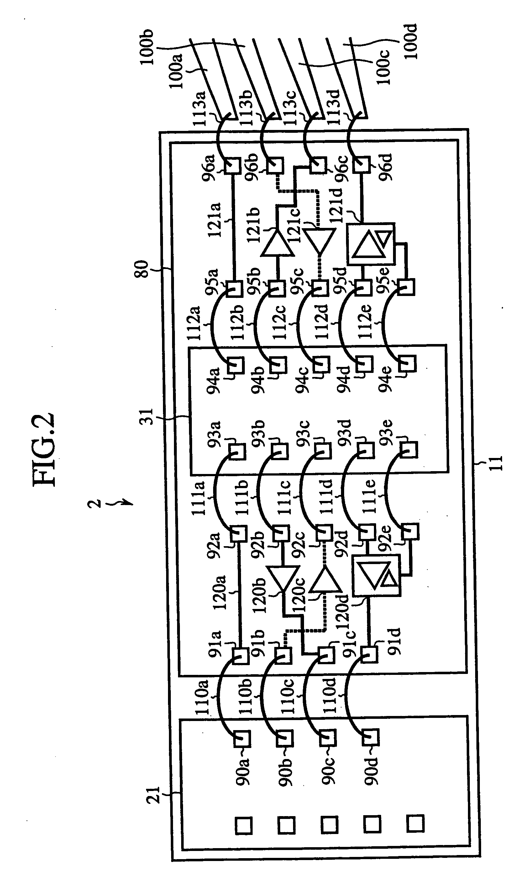
[0064]FIG. 2 is a plan view showing a semiconductor integrated circuit device according to a second embodiment of the present invention. In FIG. 2, reference numeral 2 indicates a semiconductor integrated circuit device. Reference numeral 11 indicates a bonding pad (bonding PAD), reference numeral 21 indicates a semiconductor integrated circuit chip A (Chip A) disposed on the bonding PAD 11, reference numeral 80 indicates a semiconductor integrated circuit chip (I / F Chip) including interface functions (I / F functions), which is disposed on the bonding PAD 11, and reference numeral 31 indicates a semiconductor integrated circuit chip (Chip B) disposed between portions where the I / F functions of the I / F chip80 are provided, respectively. Reference numerals 90a-90d indicate pads (PADs) of the Chip A21, reference numerals 91a-91d, 92a-92e, 95a-95e and 96a-96dindicate pads (PADs) of the I / F Chip80, and reference numerals 93a-93e and 94a-94e indicate pads (PADs) of the Chip B31, respective...
third embodiment
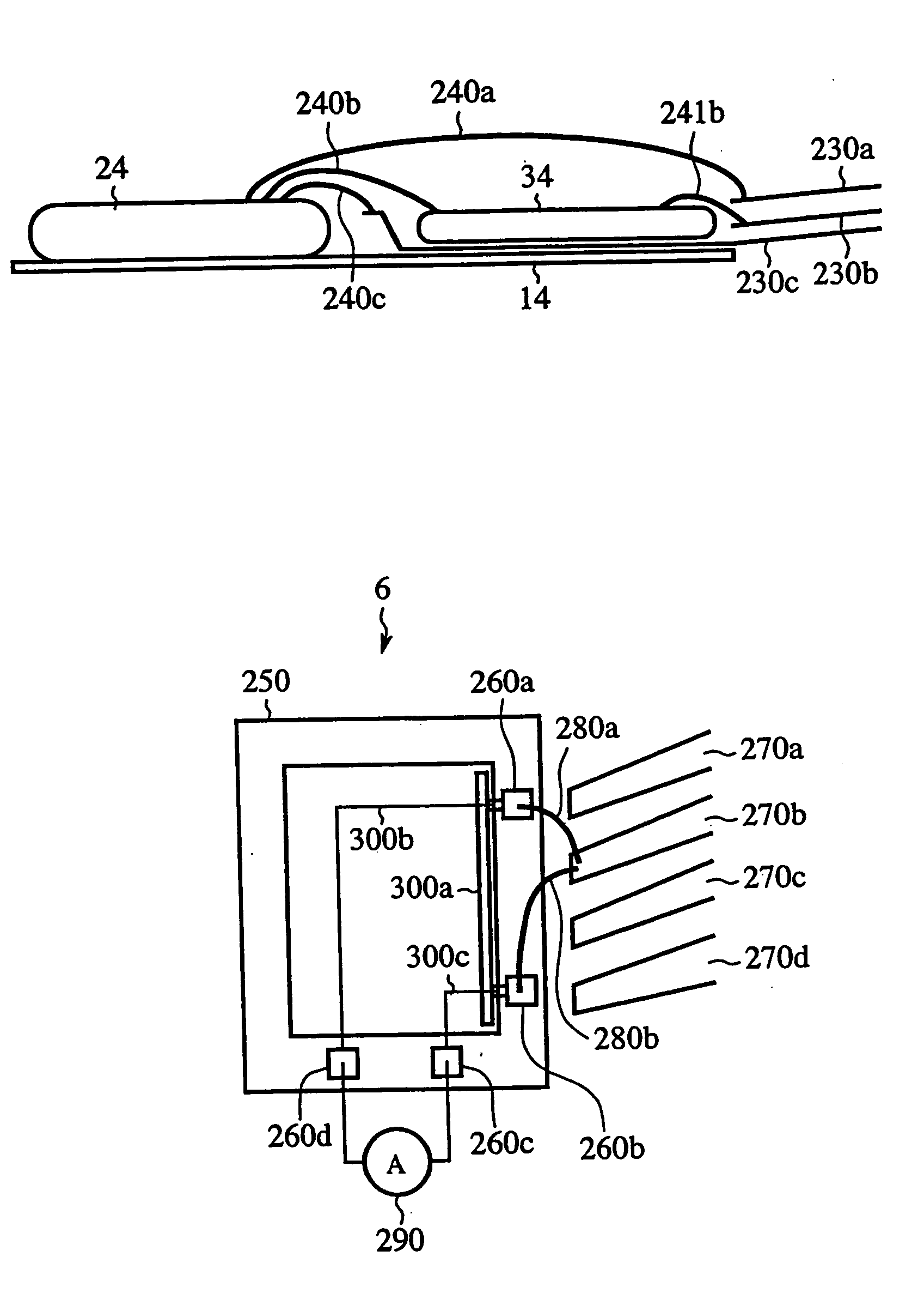
[0083]FIG. 3 is a plan view showing a semiconductor integrated circuit device according to a third embodiment of the present invention. FIG. 4 is a cross-sectional view taken along line IV-IV of FIG. 3, and FIG. 5 is a cross-sectional view taken along line V-V of FIG. 3, respectively. In FIG. 4, reference numeral 3 indicates a semiconductor integrated circuit device. Reference numeral 12 indicates a bonding pad (bonding PAD), reference numeral 22 indicates a semiconductor integrated circuit chip A (Chip A) disposed on the bonding PAD 12, reference numeral 81 indicates an I / F semiconductor integrated circuit chip (I / F Chip) including interface functions (I / F functions), which is disposed on the bonding PAD 12, reference numeral 32 indicates a semiconductor integrated circuit chip B (Chip B) disposed on the I / F chip 81, and reference numeral 130 indicates a height adjusting semiconductor integrated circuit chip (height adjustment Chip) including interface functions (I / F functions), wh...
PUM
 Abstract
Description
Claims
Application Information
 - R&D
- Intellectual Property
- Life Sciences
- Materials
- Tech Scout
- Unparalleled Data Quality
- Higher Quality Content
- 60% Fewer Hallucinations
Browse by: Latest US Patents, China's latest patents, Technical Efficacy Thesaurus, Application Domain, Technology Topic, Popular Technical Reports.
© 2025 PatSnap. All rights reserved.Legal|Privacy policy|Modern Slavery Act Transparency Statement|Sitemap|About US| Contact US: help@patsnap.com


