Semiconductor device

a technology of semiconductors and devices, applied in the direction of printed circuit non-printed electric components association, lighting and heating apparatus, domestic cooling apparatus, etc., can solve the problem of large dead space of the insulation layer, and achieve the effect of reducing the dead spa

Inactive Publication Date: 2005-07-28
AOI ELECTRONICS CO LTD
View PDF2 Cites 48 Cited by
  • Summary
  • Abstract
  • Description
  • Claims
  • Application Information

AI Technical Summary

Benefits of technology

[0007] It is, therefore, an object of the present invention to provide a semiconductor device capable of reducing a dead space formed around a semiconductor substrate such as a silicon substrate.
[0013] In the semiconductor device of this aspect, the wiring board is formed around the semiconductor substrate and the semiconductor constructing body having the external connecting electrodes. Accordingly, a dead space formed around the semiconductor substrate can be reduced.

Problems solved by technology

Therefore, when the planar size of the whole semiconductor device is to be increased by increasing the planar size of this insulating layer, the insulating layer forms a large dead space.

Method used


Image

  • Semiconductor device
  • Semiconductor device
  • Semiconductor device

Examples


first embodiment

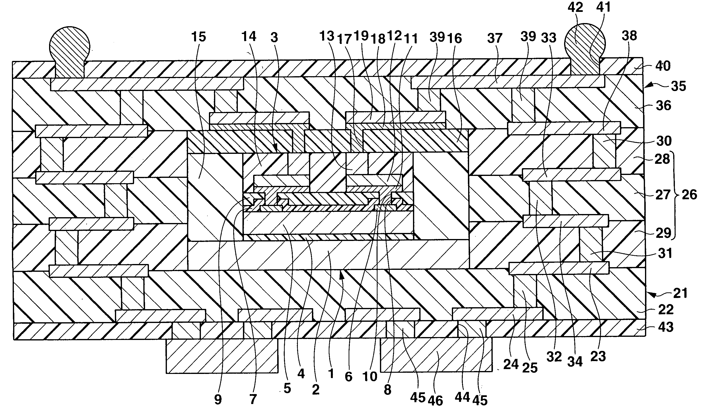
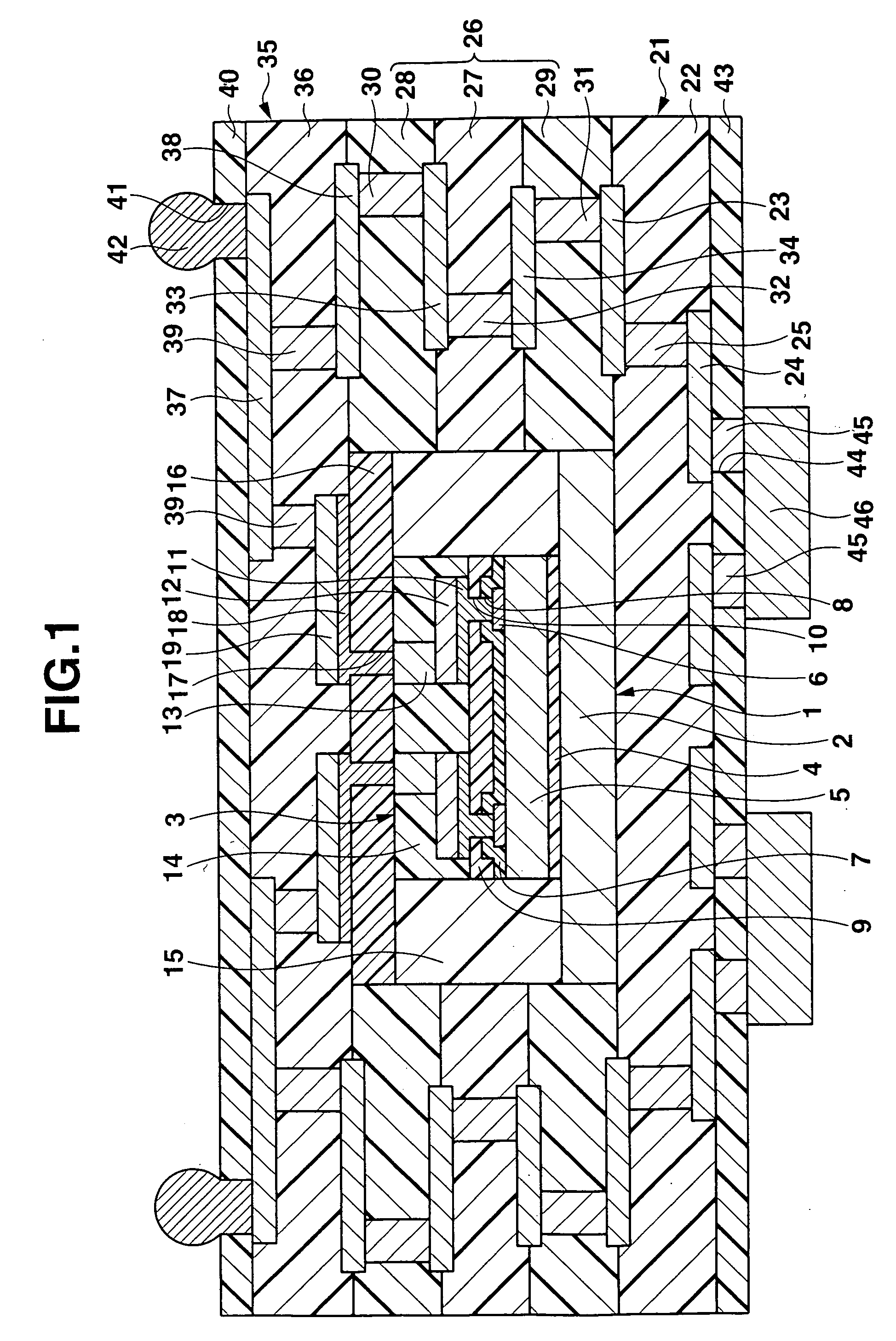
[0038]FIG. 1 is a sectional view of a semiconductor device according to the first embodiment of the present invention. This semiconductor device includes a semiconductor block 1. The semiconductor block 1 will be briefly explained below. The semiconductor block 1 has a support plate 2, semiconductor constructing body 3, insulating layer 15, upper insulating film 16, and upper interconnections 19 (second interconnections). That is, the semiconductor block 1 includes the support plate 2 having a square planar shape. The support plate 2 can be any of an insulating plate made of, e.g., resin, silicon, or ceramics, a metal plate such as a copper foil, or a prepreg material or buildup material (to be described later).

[0039] The lower surface of the semiconductor constructing body 3 having a square planar shape and a size smaller to a certain degree than the size of the support plate 2 is fixed to the upper surface of the support plate 2 via an adhesive layer 4 made of a die bonding mater...

second embodiment

[0083]FIG. 20 is a sectional view of a semiconductor device according to the second embodiment of the present invention. This semiconductor device largely differs from that shown in FIG. 1 in that a semiconductor block 1 has a structure in which an upper overcoat layer 71 made of, e.g., a solder resist is formed on the upper surface of an upper insulating film 16 including upper interconnections 19, holes 72 are formed in those portions of the upper overcoat film 71, which correspond to connecting pad portions of the upper interconnections 19, and conductive connecting portions 73 made of, e.g., metal paste are formed in the holes 72 and connected to the connecting pad portions of the upper interconnections 19. In addition, lower-surface interconnections 38 of an upper wiring board 35 are connected to the conductive connecting portions 73 of the semiconductor block 1.

[0084] In the fabrication of this semiconductor device, in a step shown in FIG. 21 which corresponds to FIG. 17 of t...

third embodiment

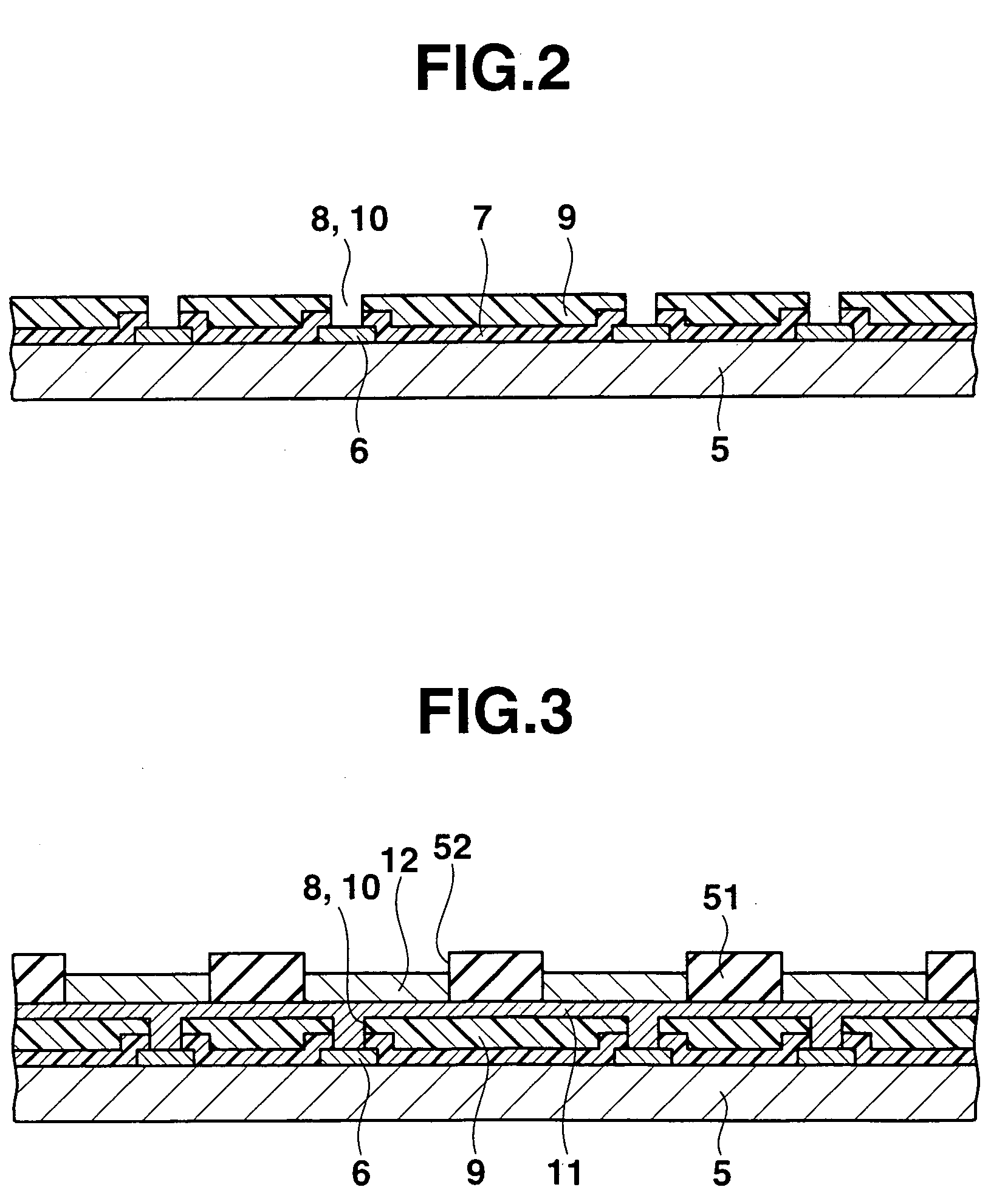
[0085] In the first and second embodiments, the semiconductor block 1 is obtained by forming the insulating layer 15 around the semiconductor constructing body 3, and the intermediate wiring board 26 is formed around the semiconductor block 1. By contrast, in the third embodiment shown in FIG. 22, an intermediate wiring board 26 is directly formed around a semiconductor constructing body 3. In the third embodiment, the area of the whole semiconductor device can be reduced by the area of the insulating layer 15 which is omitted. The rest of the arrangement of the third embodiment is the same as the first embodiment, so the same reference numerals as in the first embodiment denote the same parts, and a detailed explanation thereof will be omitted. Note that the adhesive layer 4 is omitted because when a semi-hardened support plate 2 is cured by heating and pressing, a silicon substrate 5 of the semiconductor constructing body 3 is held by the fixing force of the support plate 2. Also,...


PUM


Abstract

A semiconductor device includes a semiconductor constructing body formed on a base member, and having a semiconductor substrate and a plurality of external connecting electrodes formed on the semiconductor substrate. A wiring board is formed around the semiconductor constructing body, and has first interconnections on at least a surface thereof. Second interconnections are formed on the semiconductor constructing body and wiring board, and electrically connected to the external connecting electrodes of the semiconductor constructing body.

Description

CROSS-REFERENCE TO RELATED APPLICATIONS [0001] This application is based upon and claims the benefit of priority from prior Japanese Patent Application No. 2004-018535, filed Jan. 27, 2004, the entire contents of which are incorporated herein by reference. BACKGROUND OF THE INVENTION [0002] 1. Field of the Invention [0003] The present invention relates to a semiconductor device incorporating a semiconductor constructing body. [0004] 2. Description of the Related Art [0005] The conventional semiconductor device disclosed in Jpn. Pat. Appln. KOKAI Publication No. 2003-298005 includes solder balls as connecting terminals for external connection outside a silicon substrate. Therefore, this semiconductor device has a structure in which a silicon substrate having a plurality of connecting pads on its upper surface is formed on the upper surface of a base plate, an insulating layer is formed on the upper surface of the base plate around the silicon substrate, an upper insulating film is fo...

Claims


Application Information

Patent Timeline
Patent Type & Authority Applications(United States)
IPC IPC(8): H01L23/52H01L21/3205H01L21/48H01L21/60H01L21/68H01L23/12H01L23/31H01L23/498H01L23/538H01L25/00H01L25/04H01L25/18H05K1/18
CPCH01L21/4857H01L21/568H01L2924/0665H01L2924/014H01L2924/01006H01L2224/2919H01L24/29H01L24/27H05K1/185H01L2924/19043H01L21/6835H01L23/3114H01L23/3128H01L23/49816H01L23/49822H01L23/5389H01L24/24H01L24/82H01L24/83H01L24/97H01L2224/24226H01L2224/274H01L2224/82039H01L2224/83191H01L2224/8385H01L2224/97H01L2924/01013H01L2924/01029H01L2924/01033H01L2924/01074H01L2924/01078H01L2924/01082H01L2924/07802H01L2924/10253H01L2924/14H01L2924/15311H01L2924/19041H01L2224/82H01L2924/00H01L24/05H01L2224/05008H01L2224/05022H01L2224/05024H01L2224/05124H01L2224/05147H01L2224/05166H01L2224/05548H01L2224/05569H01L2224/056H01L2224/05647H01L2224/13022H01L2924/12042H01L2924/00014F25D3/005F25D31/003F25D2400/22F28F3/00
Inventor JOBETTO, HIROYASUMIHARA, ICHIRO
Owner AOI ELECTRONICS CO LTD
Why Eureka
Try Eureka