Fabrication method of semiconductor integrated circuit device

a technology of integrated circuit devices and fabrication methods, which is applied in the direction of inspection/indentification of circuits, instruments, image data processing, etc., can solve the problem of a significant difference of 100:1 at most in lightness value, and achieve the effect of facilitating visual confirmation of a pad, reducing the cost of preparing data, and improving the total efficiency of the devi

Active Publication Date: 2005-07-28
RENESAS ELECTRONICS CORP
View PDF4 Cites 31 Cited by
  • Summary
  • Abstract
  • Description
  • Claims
  • Application Information

AI Technical Summary

Benefits of technology

[0026] It is an object of the present invention to provide a 2D-3D inspection technique for solder printed on a substrate, which technique permits easy preparation of data and easy visual detection of a defective portion.
[0029] The present invention is applied to a method of fabricating a semiconductor integrated circuit device, comprising the steps of printing solder onto a substrate, inspecting the solder printed onto the substrate, and mounting circuit components onto the solder printed on the substrate. The inspection step comprises the steps of inspecting in 3D the solder printed on the substrate, inspecting in 2D the solder printed on the substrate, and displaying a defective portion in the 3D inspection on a larger scale in 2D. Thus, both the 2D inspecting function and the 3D inspecting function are provided, and 3D inspection is followed by 2D inspection, whereby a 2D picked-up image of a pad (printed solder) determined to be defective can be displayed on a larger scale simultaneously with the end of inspection. Hence, it is possible to provide a worker with an effective visually confirmed environment at the time.
[0032] It is possible to provide a 2D-3D inspection technique for solder printed on a substrate, which technique can omit manual inspection data preparing work so as to reduce the cost for preparing data and facilitate a visual confirmation of a pad that has been determined to be defective, thereby improving the total efficiency thereof as a man-machine system and reducing the operation cost.

Problems solved by technology

In applying 3D inspection to a solder print inspection device, a difficult problem is encountered in that an actual object to be inspected often involves substrate that is warped that, between an upper surface of the printed solder and the substrate surface (resist surface), there is a significant difference of about 100:1 at most in terms of the lightness value on an area image of a slit light-applied portion.

Method used


Image

  • Fabrication method of semiconductor integrated circuit device
  • Fabrication method of semiconductor integrated circuit device
  • Fabrication method of semiconductor integrated circuit device

Examples


Embodiment Construction

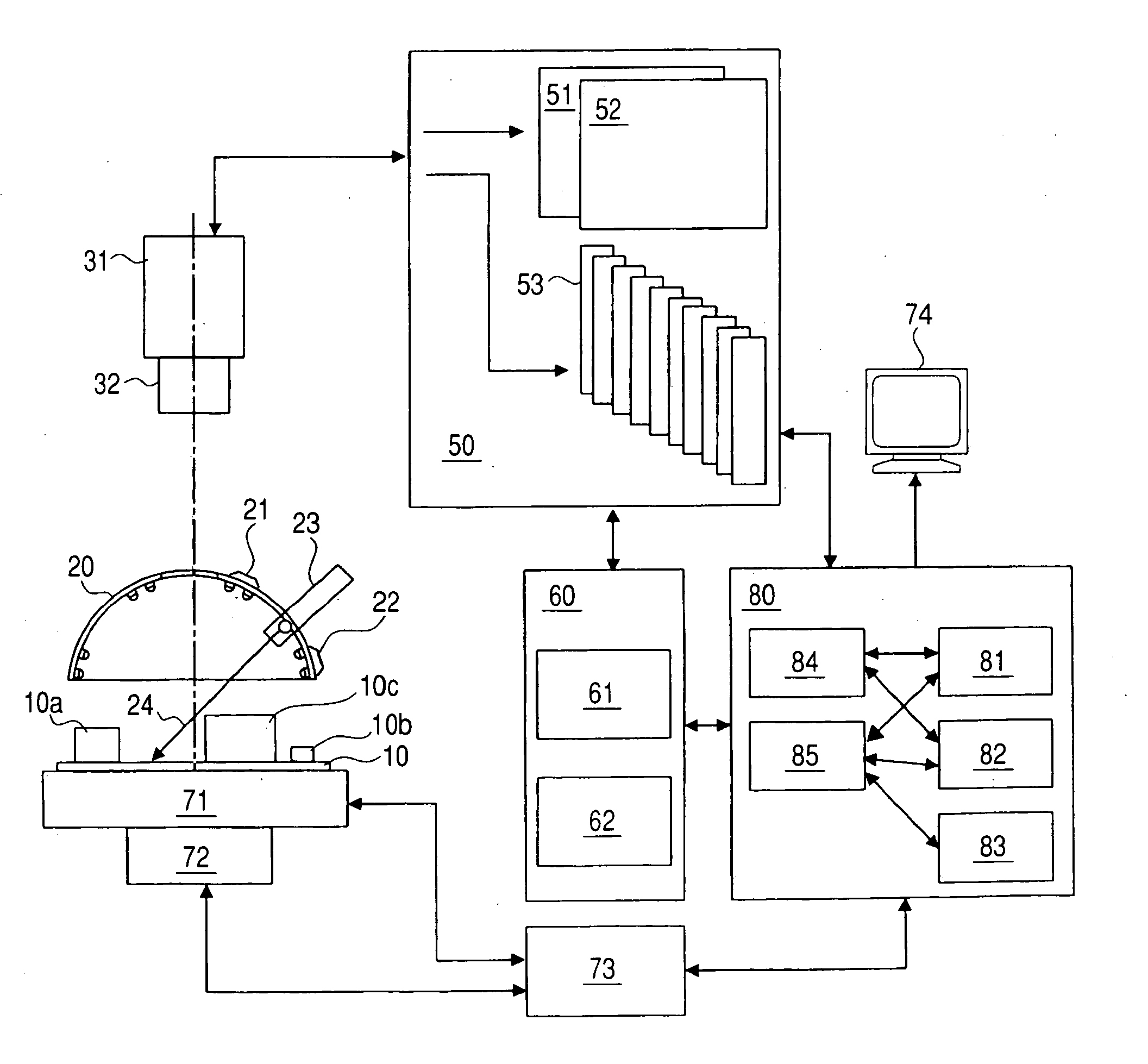
[0068] In the following description of the embodiments, the same or similar parts will be identified by the same reference numerals, and repeated explanations thereof will be omitted in principle except where required.

[0069] Where required for convenience' sake, the subject matter of this invention will be described in a divided manner into plural sections or embodiments, but unless otherwise mentioned, they are not unrelated to each other, but are in a relation such that one is a modification, a detailed description, or a supplementary explanation, of part or the whole of the other.

[0070] In the following description of the embodiments, when reference is made to a number of elements (including the number, numerical value, quantity, and range), no limitation is made to the number referred to, but numerals above and below the number referred to will do as well, unless otherwise mentioned, and except for the case where it is basically evident that a limitation is made to the number ...


PUM

PropertyMeasurementUnit
lengthaaaaaaaaaa
lengthaaaaaaaaaa
sizeaaaaaaaaaa

Abstract

In the fabrication of a semiconductor integrated circuit device, a 2D-3D inspection technique for solder printed on a substrate is provided which permits easy preparation of data and easy visual confirmation of a defective portion. In a substrate inspecting step first, a 3D inspection is performed, followed by execution of 2D inspection, whereby a 2D picked-up image of the portion of a pad determined to be defective can be displayed on a larger scale simultaneously with the end of inspection, thereby providing an environment for efficient visual confirmation of the defect. Further, by subjecting a raw substrate to measurement at the time of preparing inspection data, a relation between an original height measurement reference generated automatically by the inspection system and the height of a pad upper surface is checked, whereby it is possible to measure the height and volume of printed solder based on the pad upper surface.

Description

CROSS-REFERENCE TO RELATED APPLICATION [0001] The present application claims priority from Japanese patent application No. 2004-015718, filed on Jan. 23, 2004, the content of which is hereby incorporated by reference into this application. BACKGROUND OF THE INVENTION [0002] The present invention relates in general to a technique for use in fabricating a semiconductor integrated circuit device; and, more particularly, the invention relates to a technique applicable effectively to an inspection process in which solder printed on a substrate is inspected in three dimensions (hereinafter referred to as “3D”) and in two dimensions (referred to as “2D” hereinafter). [0003] For example, in connection with the fabrication of a semiconductor integrated circuit device, solder inspecting techniques are described in Japanese Unexamined Patent Publication No. 2000-193432 (Patent Literature 1) and No. 2000-22326 (Patent Literature 2). [0004] Patent Literature 1, in connection with a technique for...

Claims


Application Information

Patent Timeline
Patent Type & Authority Applications(United States)
IPC IPC(8): G01N21/956G01B11/00G06T1/00H05K1/02H05K3/34
CPCG01N21/95684G01N2021/95646H05K1/0269H05K3/3452H05K3/3484H05K2203/163H01L2924/13091H01L2224/73204H01L2924/15311H01L2924/00H05K3/3485H01L2224/32225H01L2224/16225G01N21/00
Inventor WATANABE, NORIO
Owner RENESAS ELECTRONICS CORP
Why Eureka
Try Eureka