Method and system for batch forming spring elements in three dimensions

a technology of spring elements and three dimensions, applied in the field of three-dimensional spring element forming, can solve the problems of increasing lead count, prohibitively difficult and expensive to use conventional techniques to make separable electrical connections to these semiconductor devices, and shrinking package geometries,

Inactive Publication Date: 2005-07-28
NEOCONIX INC
View PDF99 Cites 78 Cited by
  • Summary
  • Abstract
  • Description
  • Claims
  • Application Information

AI Technical Summary

Problems solved by technology

Advances in electronic device packaging technology have led to shrinking package geometries and increasing lead count.
At the 250 micron pitch level, it is prohibitively difficult and expensive to use conventional techniques to make separable electrical connections to these semiconductor devices.
The problem is becoming even more critical as the pitch of contact pads on a semiconductor device decreases below 50 microns and simultaneous connection to multiple contact pads in an array is required.
In particular, the mechanical, electrical, and reliability performance criteria of an interconnect system are becoming increasingly demanding.
Conventional interconnect technologies have not been able to meet all of the mechanical, electrical, and reliability requirements for use with high speed, small dimension, and large pin count IC devices.
A particular problem encountered by today's interconnect systems is the variation in coplanarity (vertical offset) and positional misalignment of the leads in the electronic components to be connected.
In a conventional LGA package, the pads (the leads) of the package can become non-planar due to substrate warping.
When the amount of the resulting vertical offset exceeds the tolerance of a LGA connector, some of the pads may not be able to make electrical contact with the connector at all.
Planarity variations of the pads of an LGA component make it difficult to make high quality and reliable electrical connections to all the leads of the electronic component.
Moreover, the location of the leads may also deviate from their predefined ideal position due to manufacturing limitations, resulting in positional misalignment.
Planarity problems are not limited to IC packages but may also exist on the printed circuit board (PCB) to which these IC packages are attached.
Planarity problems may exist for LGA pads formed as an area array on a PCB due to warping of the PCB substrate.
While LGA connectors can be effectively used to electrically connect an LGA package to printed circuit boards or modules, the connector interface between the connector and the component to be connected are subject to potential reliability degradation.
For instance, corrosive materials or particulate debris can enter the interface area, preventing a proper electrical connection from being made.
Also, the repeated mating and separation of an LGA package may degrade the LGA connector, causing intermittent connection conditions and inhibit reliable electrical connection.
However, when conventional approaches are used to make electrical contact to solder balls, the solder balls may be damaged or dislodged from the package. FIG. 2a illustrates the existing contact element 100 being applied to contact a solder ball 200 formed on a substrate 202.
The presence of the void 214 can affect the electrical characteristics of the connection and more importantly, degrades the reliability of the connection.
Conventional interconnect devices, such as stamped metal springs, bundled wire, and injection molded conductive adhesives, become difficult to manufacture as the dimensions are scaled down.
Stamped metal spring elements, in particular, become brittle and difficult to manufacture as the dimensions are scaled down, rendering them unsuitable for accommodating electronic components with normal positional variations.
At this size, spring elements made by existing manufacturing technologies become even more brittle and less elastic and cannot accommodate normal variations in system coplanarity and positional misalignments with a reasonable insertion force of about 30 to 40 grams per contact.
Existing methods and systems of forming spring elements in three dimensions have utilized custom tools, which are often designed for a specific size spring element, are not configurable, and are expensive to manufacture.

Method used


Image

  • Method and system for batch forming spring elements in three dimensions
  • Method and system for batch forming spring elements in three dimensions
  • Method and system for batch forming spring elements in three dimensions

Examples


Embodiment Construction

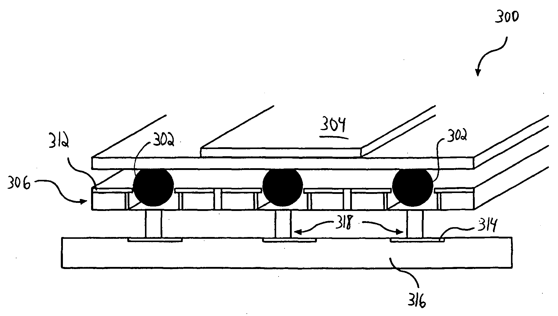
[0066]FIGS. 3a and 3b are cross-sectional views of a beam ball grid array (BBGA) system constructed in accordance with the present invention. In the first construction 300 illustrated in FIG. 3a, solder balls 302 provide a method of establishing an electrical contact between the device, packages, or module 304, and a carrier 306. The solder balls 302 are shown disposed within plated through holes or vias 308 that have been fabricated into the carrier 306 by printed circuit techniques. The solder balls 302 are given elasticity by virtue of their suspension upon flexible contact arms 310 formed as part of a layer 312. The contact arms 310 cradle the solder ball 302, as shown in FIG. 3e, and provide a spring-like support as shown in FIGS. 3c and 3d.

[0067] An array of contact arms 310 is fabricated in layer 312, as better observed with reference to FIG. 3f. Different design patterns for the contact arms 310 are respectively illustrated by elements 310a, 310b, 310c, and 310d in FIG. 3g....


PUM


Abstract

A system for batch forming a sheet of spring elements in three dimensions includes a top spacer layer. A plurality of ball bearings is arranged in a predetermined pattern on the top spacer layer. A spring element sheet containing the spring elements defined in two dimensions is positioned on the top spacer layer and the plurality of ball bearings. A top spacer layer is positioned on the spring element sheet. The top spacer layer and the bottom support layer are adapted to have a force applied thereto to push the plurality of ball bearings against the spring element sheet, such that the spring elements extend above the plane of the spring element sheet, thereby forming the spring elements in three dimensions.

Description

[0001] This application is a continuation-in-part of U.S. patent application Ser. No. 10 / 412,729, filed Apr. 11, 2003, which is herein incorporated by reference in their entirety. [0002] This application also claims the benefit of U.S. Provisional Application No. 60 / 554,816, filed Mar. 19, 2004, and International Application No. US04 / 011074, Filed Apr. 9, 2004, both of which are herein incorporated by reference in its entirety.BACKGROUND [0003] 1. Field of the Invention [0004] The present invention relates to forming spring elements in three dimensions, and more particularly, to a method and system for batch forming spring elements in three dimensions using a configurable die. [0005] 2. Background of the Invention [0006] Electrical interconnects or connectors are used to connect two or more electronic components together or to connect an electronic component to a piece of electrical equipment, such as a computer, router, or tester. The term “electronic component” includes, but is no...

Claims


Application Information

Patent Timeline
Patent Type & Authority Applications(United States)
IPC IPC(8): H01L23/32H01L23/48H01R12/04H01R13/03H01R13/24H01R43/00H01R43/20H05K3/32H05K3/40H05K7/10
CPCH01L23/32H01L24/72H01L2924/10253H01L2924/01004H01L2924/01005H01L2924/01013H01L2924/01015H01L2924/01029H01L2924/01074H01L2924/01078H01L2924/01079H01L2924/01082H01L2924/14H01L2924/19041H01L2924/19042H01L2924/19043H01L2924/30107H01L2924/3011H01R13/03H01R13/2407H01R13/2492H01R43/007H01R43/205H05K3/326H05K3/4092H05K7/1069H01R12/52H01R12/714H01L2924/01006H01L2924/01019H01L2924/01024H01L2924/01033H01L2924/00
Inventor RADZA, ERIC M.WILLIAMS, JOHN D.
Owner NEOCONIX INC
Why Eureka
Try Eureka