Chip packaging module with active cooling mechanisms

a technology of active cooling and packaging module, which is applied in the direction of solid-state devices, basic electric elements, electrical apparatus construction details, etc., can solve the problems of insufficient heat transfer path and inadequate current approach to packaging such high-power chips, and achieve high-efficiency effects

Inactive Publication Date: 2005-08-04
IBM CORP
View PDF7 Cites 51 Cited by
  • Summary
  • Abstract
  • Description
  • Claims
  • Application Information

AI Technical Summary

Problems solved by technology

The current approach to packaging such higher power chips becomes inadequate because the heat generated on the active side of the chip has to pass through the chip, the chip-to-package interface, the package cover, and then to the heat sinking device.
The heat transfer path is not efficient enough.

Method used


Image

  • Chip packaging module with active cooling mechanisms
  • Chip packaging module with active cooling mechanisms
  • Chip packaging module with active cooling mechanisms

Examples


Embodiment Construction

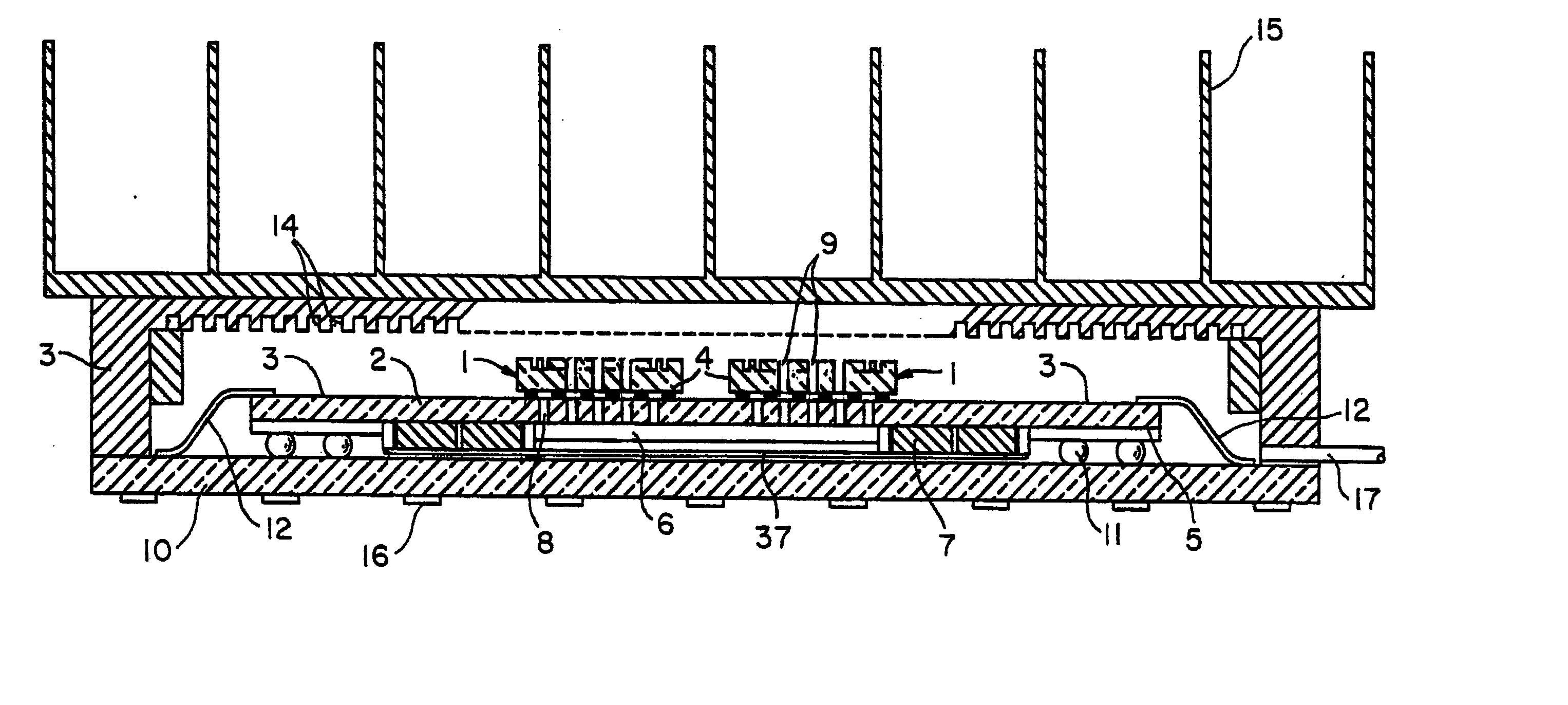
[0016] The invention is illustrated in connection with a common in the art multichip type module with the addition of the invention of a built in active cooling mechanism as is shown in a cross-sectional view in FIG. 1 and subsequent figures.

[0017] Referring to FIG. 1, thin film chips labelled 1, of which two are shown, are mounted on an insulating or semiconducting supporting substrate labelled 2 made of silicon, ceramic or other such material with or without thin-film wiring layers, not shown, on the upper surface 3. The chips 1 themselves, have a surface through which contacts are made, an adjacent heat generating region and a heat radiating or back side surface with grooves for increased surface area for improved heat transfer. The distance between the heat generating region and the heat radiating surface attenuates heat transfer away from the chip. A minimum thickness of the order of 50-100 micrometers between the heat generating region and the heat radiating surface is prefer...


PUM


Abstract

The invention is directed to structure and methods of improving the cooling capacity of chip packaging modules. The chip packaging module has a substrate with thin-film wiring on one side and grooves or channels etched on one or both sides where coolant pumps are embedded. The coolant pumps are used to enhance the liquid flowing inside the module. The coolant flows through the chips within the vias in the chips or around the chips when the chips do not have vias. Both cooling modes, single or two-phase modes can be adopted in the module.

Description

FIELD OF THE INVENTION [0001] The invention is in the field of heat dissipation from semiconductor chips where those semiconductor chips are packaged in a modular housing and in particular to fluid enhanced heat transfer within the housing. BACKGROUND AND RELATION TO THE PRIOR ART [0002] It is well known that the power and power density of semiconductor chips are increasing rapidly. The current approach to packaging such higher power chips becomes inadequate because the heat generated on the active side of the chip has to pass through the chip, the chip-to-package interface, the package cover, and then to the heat sinking device. The heat transfer path is not efficient enough. A need is becoming apparent that a new chip packaging approach having a more efficient heat transfer will be required. [0003] There has been some work in the art in chip packaging where chips are thinned to thicknesses even less than about 100 micrometers and the use of such thinned chips in systems that combi...

Claims


Application Information

Patent Timeline
Patent Type & Authority Applications(United States)
IPC IPC(8): H01L23/427H01L23/473H02B1/00H05K7/20
CPCH01L23/427H01L23/473H01L2224/16225H01L2224/48091H01L2924/10158H01L2924/00014
Inventor MOK, LAWRENCE SHUNGWEIBUCHWALTER, LEENA PAIVIKKIBUCHWALTER, STEPHEN LESLIE
Owner IBM CORP
Why Eureka
Try Eureka