Display panel and method for manufacturing display panel

Inactive Publication Date: 2005-08-11
SANYO ELECTRIC CO LTD
View PDF7 Cites 25 Cited by
  • Summary
  • Abstract
  • Description
  • Claims
  • Application Information

AI Technical Summary

Benefits of technology

[0010] According to the present invention, a pixel substrate and a sealing substrate are joined through welding by laser irradiation. With this structure, it is possible to achieve reliable sealing with a small area, which allows for an increase in an area of the display region in which the display can actually be realized and a smaller display size. In addition, because the joining

Problems solved by technology

However, because the terminal and line are typically made of a metal such as aluminum and does not allow l

Method used


Image

  • Display panel and method for manufacturing display panel
  • Display panel and method for manufacturing display panel
  • Display panel and method for manufacturing display panel

Examples


Embodiment Construction

[0020] A preferred embodiment (hereinafter, referred to simply as “embodiment”) of the present invention will now be described referring to the drawings.

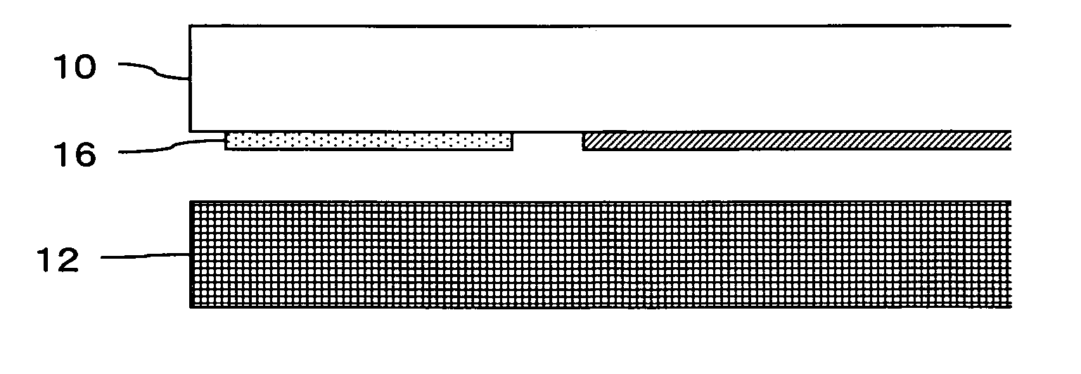
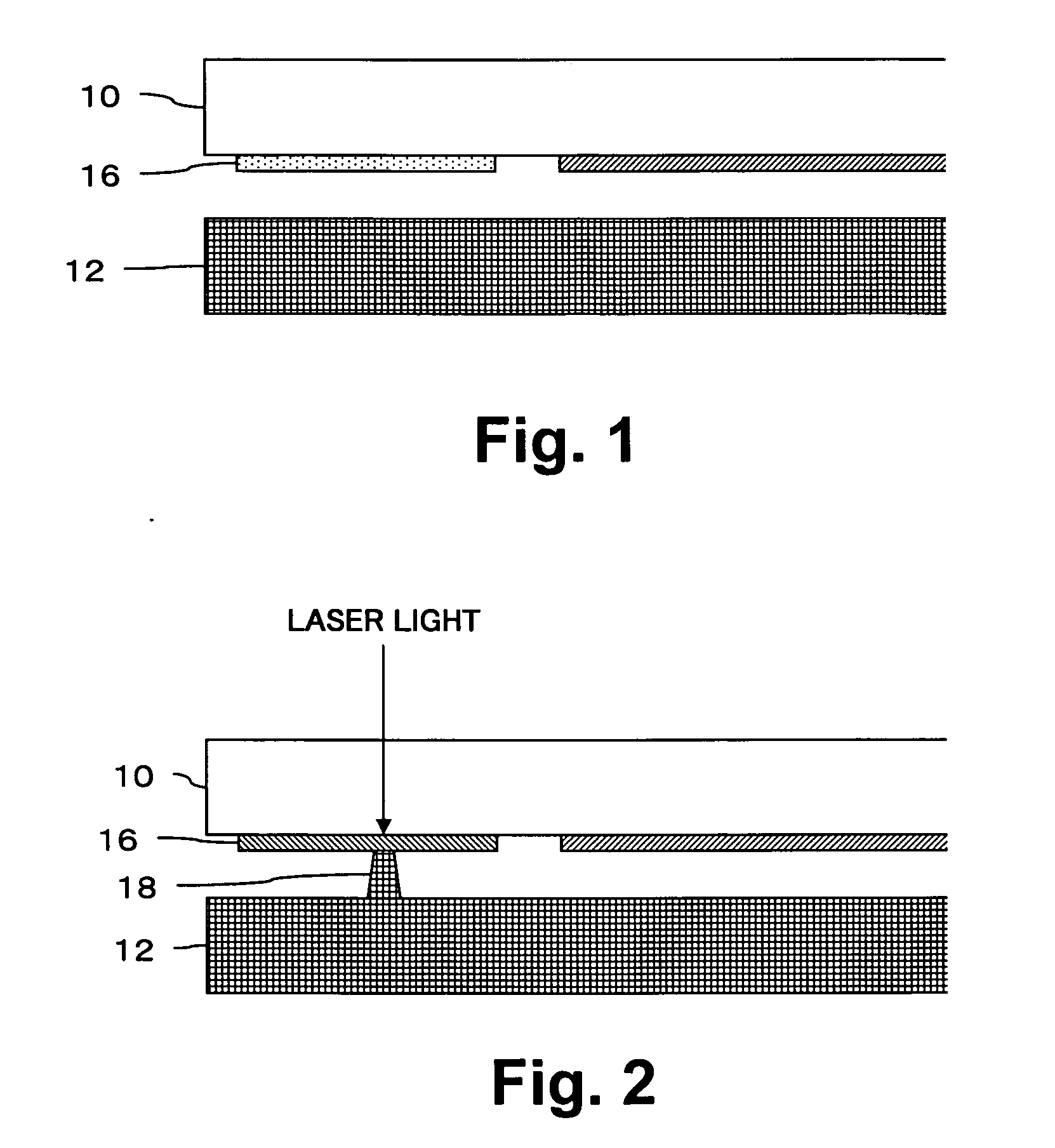
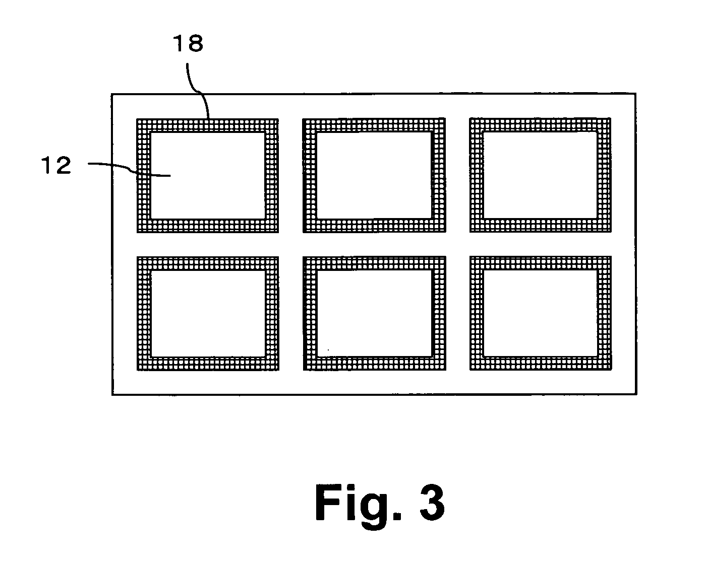
[0021]FIGS. 1 and 2 show joining of substrates according to a preferred embodiment of the present invention. An EL substrate 10 which is a pixel substrate on which a pixel or pixels are formed and a sealing substrate 12 for sealing an upper surface of the EL substrate 10 are placed opposing each other. The sealing substrate 12 is made of an absorbing structure which absorbs laser, such as nontransparent glass. Here, the entire region of the sealing substrate 12 need not be nontransparent, but it is necessary that the portion to be welded functions as an absorbing structure. For example, the sealing substrate 12 can be made nontransparent by doping a metal though an ion injection or ion exchange method, for example, and the nontransparent substrate 12 functions as an absorbing structure. In the ion exchange method, a resist which is...


PUM

PropertyMeasurementUnit
Transparencyaaaaaaaaaa

Abstract

A sealing substrate is placed opposing an EL substrate with a predetermined gap therebetween. The sealing substrate is nontransparent. A laser irradiation region of a terminal portion of the EL substrate is formed by a transparent conductor such as ITO. With this structure, a periphery region of the sealing substrate is irradiated with laser through the EL substrate and heated, so that glass is elevated and welded.

Description

CROSS-REFERENCE TO RELATED APPLICATIONS [0001] The entire disclosure of Japanese Patent Application No. 2004-9872 including specification, claims, drawings and abstract is incorporated herein by reference. BACKGROUND OF THE INVENTION [0002] 1. Field of the Invention [0003] The present invention relates to manufacture of a display panel such as an organic electroluminescence (hereinafter simply referred to as “EL”) display panel and, in particular, to a sealing structure in the display panel. [0004] 2. Description of the Related Art [0005] Plasma display panels (PDP) and liquid crystal display devices (LCD) are becoming widely available as thin flat display panels and organic EL panels are commercially available. [0006] In an organic EL panel, an organic material is used as a light emitting material in each pixel or the like. Because the lifetime of the organic material is shortened when the organic material contains moisture, it is necessary to minimize an amount of moisture in a sp...

Claims


Application Information

Patent Timeline
IPC IPC(8): B23K26/18H05B33/04G09F9/30H01J1/62H01L27/32H01L51/50H01L51/52H01L51/56H05B33/02H05B33/10H05B33/14H05B33/28
CPCB23K26/18B23K2201/40B23K26/009H01L51/5237H01L51/56H01L27/3244B23K2101/40H10K59/12H10K50/841H10K50/846H10K71/00H05B33/10G09F9/30H05B33/04
Inventor NISHIKAWA, RYUJIOMURA, TETSUJI
Owner SANYO ELECTRIC CO LTD
Why Eureka
Try Eureka