Method of forming a device by removing a conductive layer of a wafer

a technology of conductive layer and wafer, applied in the direction of microstructural device, acceleration measurement using interia force, instruments, etc., can solve the problems of stiction in compliant structures, create fabrication inefficiencies, harm metallization and pre-formed circuits, etc., and achieve the effect of facilitating the removal of the intermediate layer

Active Publication Date: 2005-08-11
ANALOG DEVICES INC
View PDF8 Cites 17 Cited by
  • Summary
  • Abstract
  • Description
  • Claims
  • Application Information

AI Technical Summary

Benefits of technology

[0007] In illustrative embodiments, the first and second conductive layers form a variable capacitor that fluctuates as the first conductive layer moves. Moreover, the cavity may be sealed to have a cavity pressure that is less than atmospheric pressure. Among other materials, the first and second conductive layers may be a silicon based material (e.g., silicon, polysilicon, or silicon germanium).
[0008] The method may add circuitry to the wafer before removing the intermediate conductive layer. Among other things, the circuitry may be capable of detecti

Problems solved by technology

Such etches, however, can create fabrication inefficiencies.
Specifically, HF etches can harm metallization and pre-formed circuits, while causi

Method used


Image

  • Method of forming a device by removing a conductive layer of a wafer
  • Method of forming a device by removing a conductive layer of a wafer
  • Method of forming a device by removing a conductive layer of a wafer

Examples


Embodiment Construction

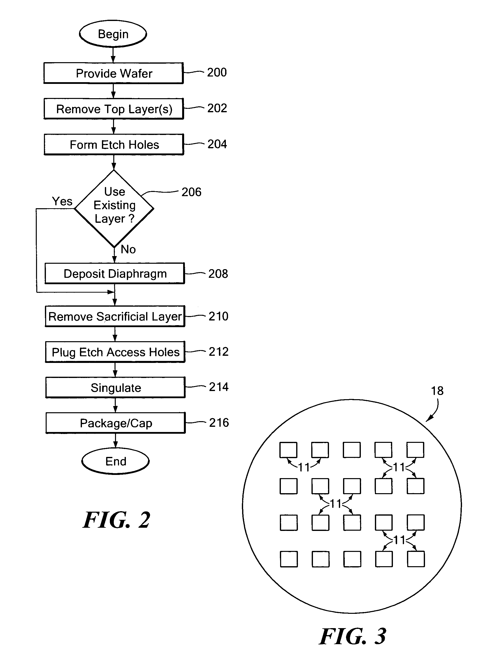
[0020] Illustrative embodiments of the invention fabricate a MEMS device (e.g., a pressure sensor) from existing layers of a multilayered wafer. Such embodiments typically use one or more conductive layers as a sacrificial layer. Details of illustrative embodiments are discussed below.

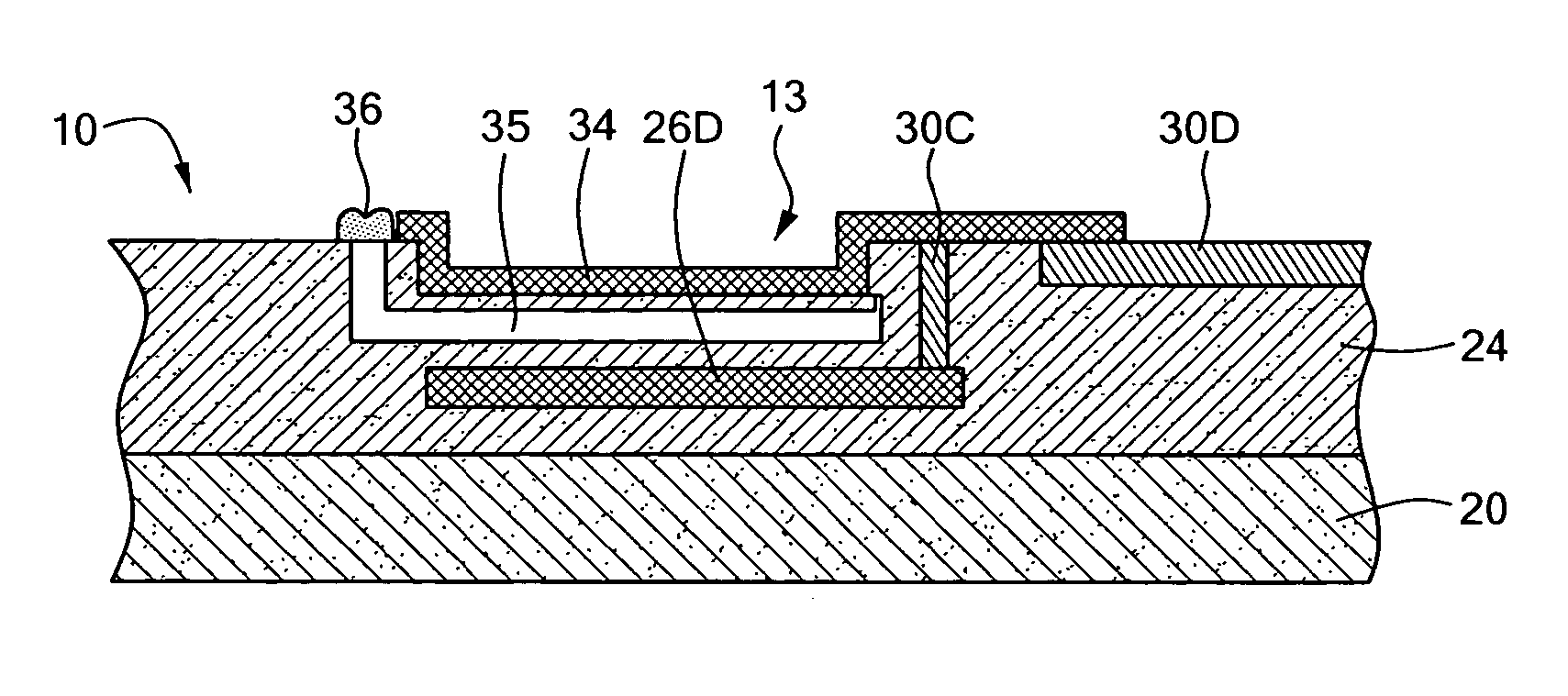
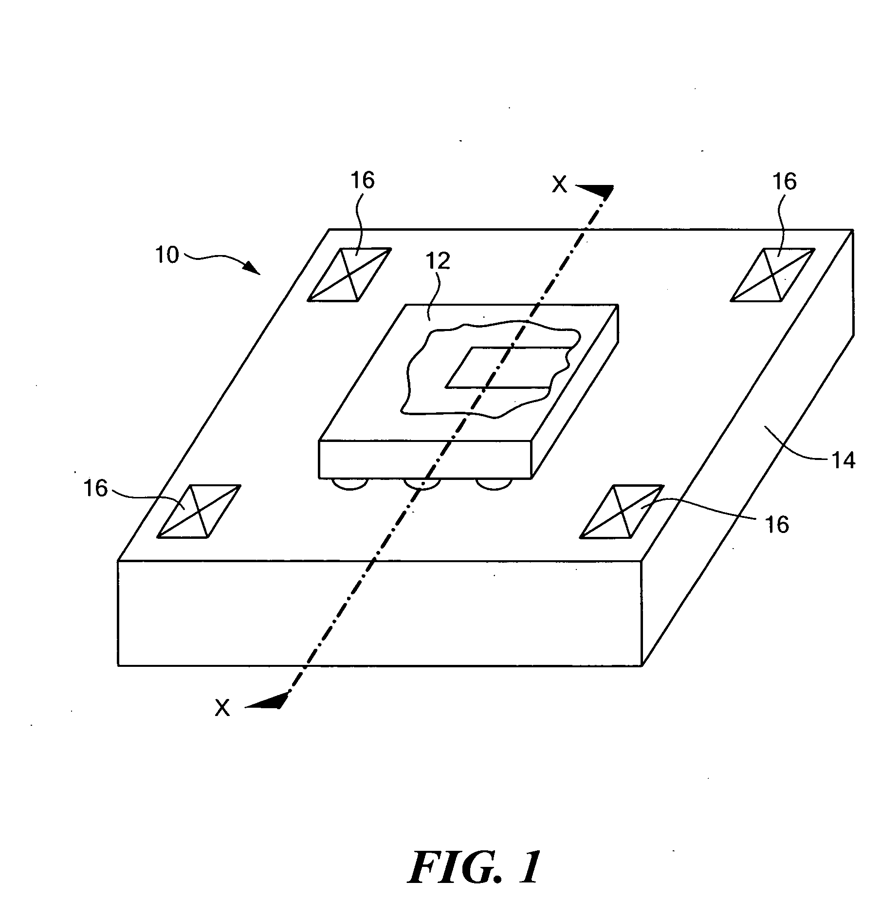
[0021]FIG. 1 schematically shows an exemplary use of a chip 10 produced in accordance with illustrative embodiments of the invention. Specifically, the chip 10 in this embodiment is a MEMS device having both circuitry 11 and movable structure 13 (see FIGS. 3, 4A-4C, and 5A-5D). The MEMS device 10 illustratively is formed on a silicon wafer and packaged within a conventional package 12. The package 12 is coupled with a circuit board 14 having interconnects 16 to electrically communicate with an external device, such as a computer.

[0022] Since it is implemented as a MEMS device, the chip 10 may execute any conventionally known functionality commonly implemented by a MEMS device, such as a pressure sens...


PUM


Abstract

A method of forming a MEMS device provides a wafer having a base, a first conductive layer, a second conductive layer, and an intermediate conductive layer. After it provides the wafer, the method removes at least a portion of the intermediate conductive layer to form a cavity between the first and second conductive layers. At least a portion of the first conductive layer is movable relative to the base to form a diaphragm, while the second conductive layer is substantially immovable relative to the base. After it forms the cavity, the method seals the cavity.

Description

PRIORITY [0001] This patent application claims priority from Provisional U.S. Patent Application No. 60 / 543,059, attorney docket numbers 2550 / 199 and APD2570-1-US, filed Feb. 9, 2004, entitled, “PRESSURE SENSOR,” and naming Timothy J. Brosnihan, Robert Sulouff, and John M. Sledziewski as inventors, the disclosure of which is incorporated herein, in its entirety, by reference.FIELD OF THE INVENTION [0002] The invention generally relates to MEMS devices and, more particularly, the invention relates to MEMS pressure sensors. BACKGROUND OF THE INVENTION [0003] Microelectromechanical systems (“MEMS,” hereinafter “MEMS devices”) are used in a wide variety of applications. For example, MEMS devices currently are implemented as microphones to convert audible signals to electrical signals, as gyroscopes to detect pitch angles of airplanes, and as pressure sensors to detect changes in pressure. In simplified terms, such MEMS devices typically have a movable structure suspended from a substrat...

Claims


Application Information

Patent Timeline
IPC IPC(8): B81B3/00
CPCB81B2201/0264B81B2203/0127B81C1/00182B81C1/00047B81B2203/0315
Inventor BROSNIHAN, TIMOTHY J.SULOUFF, ROBERT E. JR.SLEDZIEWSKI, JOHN M.
Owner ANALOG DEVICES INC
Why Eureka
Try Eureka