
LDMOS transistor with improved ESD protection

a technology of ldmos transistor and protection device, which is applied in the direction of semiconductor/solid-state device details, semiconductor devices, electrical apparatus, etc., can solve the problems of discharge path, damage to field oxide region, and scaled-down devices and thin gate oxides are more vulnerable to esd stress

Inactive Publication Date: 2005-08-18
VANGUARD INTERNATIONAL SEMICONDUCTOR CORPORATION
View PDF3 Cites 30 Cited by
  • Summary
  • Abstract
  • Description
  • Claims
  • Application Information

AI Technical Summary

Benefits of technology

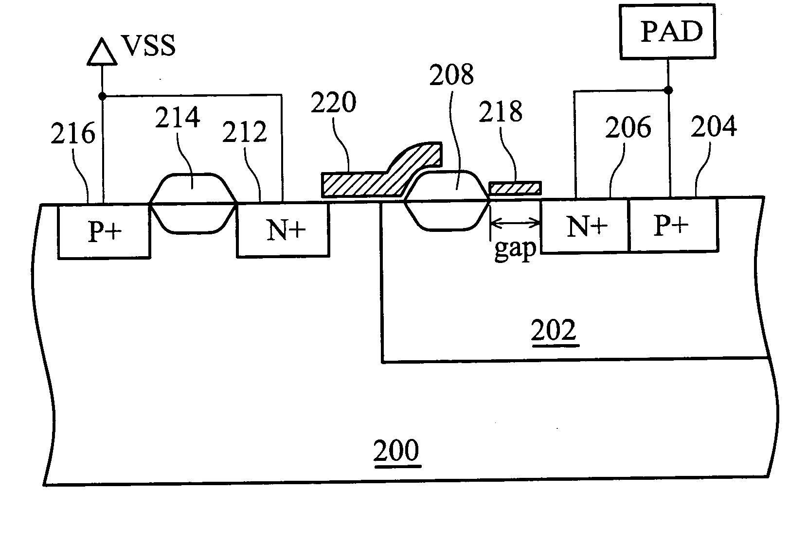
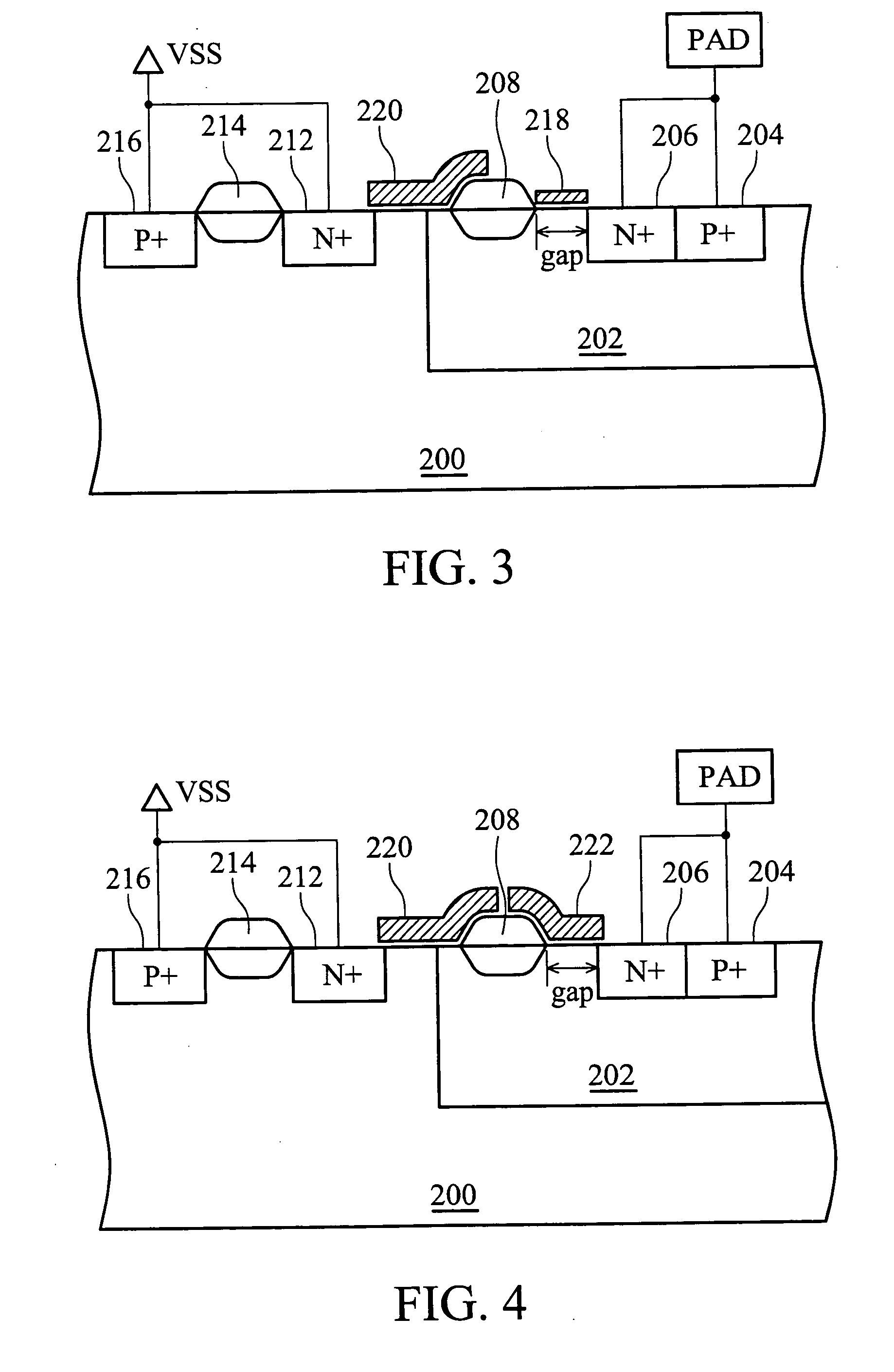
[0012] The ESD protection device according to the present invention comprises a first substrate of a first conductive type, a well of a second conductive type, a first doped region of the second conductive type, a gate, a second doped region of the third conductive type, a field oxide region, and a gap. The well and the first doped region are formed in the substrate. The gate controls the electrical connection of the first doped region and the well. A field effect transistor comprises the gate, the first doped region, and the well. The second doped region, field oxide region, and gap are formed in the well. The field oxide region is located between the gate and the second doped region. The gap is located between the field oxide region and the second doped region. The first and the third conductivity types can be either N or P type. The second conductivity type can be either P or N type.

Problems solved by technology

As the semiconductor manufacturing process develops, ESD protection has become one of the most critical reliability issues for integrated circuits (IC).
In particular, as semiconductor process advances into the deep sub-micron stage, scaled-down devices and thinner gate oxides are more vulnerable to ESD stress.
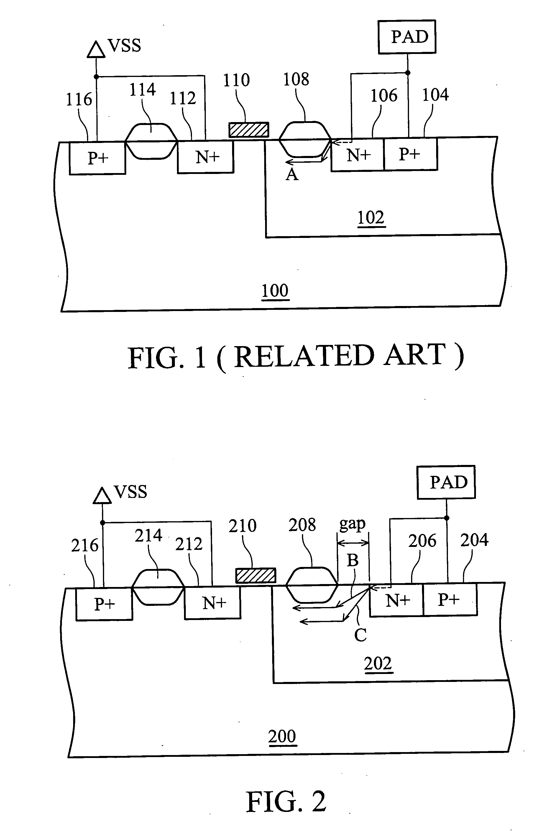
Since the secondary ESD current stays large, the change in direction generates a higher temperature in the turning point, easily damaging the field oxide region 108 and the discharge path.

Method used


Image

  • LDMOS transistor with improved ESD protection
  • LDMOS transistor with improved ESD protection
  • LDMOS transistor with improved ESD protection

Examples


Embodiment Construction

[0019]FIG. 2 is a cross-section of an ESD protection device according to a first embodiment of the present invention. The ESD protection device is an N-type LDMOS field effect transistor. The NMOS comprises gate 210, N+ region 212, and N well 202. N+ region 212 is a source of the NMOS and N well 202 a drain of the NMOS. An N+ region 206 formed in the N well 202 acts as an electrical contact for the N well 202. The gate 210 controls the electrical connection of N+ region 212 and the N well 202, and is also coupled to a grounded line VSS or pre-driver according to circuit requirements.

[0020] The P substrate 200 is coupled to the grounded line VSS through a P+ region 216. The drain is coupled to a pad through the N+ region 206.

[0021] A field oxide region 214 isolates the N+ region 212 from P+ region 216. In order to protect a gate-oxide layer under the gate 210 from overstress, a field oxide region 208 is formed between an N+ region 206 and gate 210 isolating the gate 210 from N well...


PUM


Abstract

An ESD protection device. The ESD protection device is incorporated with a gap structure in a laterally diffused metal oxide semiconductor (LDMOS) field effect transistor, isolating a doped region and a field oxide region. When a parasitical semiconductor controlled rectifier (SCR) of LDMOS is turned off, ESD current is discharged distributively through several discharge paths, avoiding ESD current focus in a signal narrow discharge path and the danger therefrom.

Description

BACKGROUND OF THE INVENTION [0001] 1. Field of the Invention [0002] The present invention relates to a protection device, and more particularly, to a high voltage electrostatic discharge (ESD) protection device. [0003] 2. Description of the Related Art [0004] As the semiconductor manufacturing process develops, ESD protection has become one of the most critical reliability issues for integrated circuits (IC). In particular, as semiconductor process advances into the deep sub-micron stage, scaled-down devices and thinner gate oxides are more vulnerable to ESD stress. Generally, the input / output pads on IC chips must at least sustain 2 kVolt ESD stress of high Human Body Mode (HBM) or 200 V of Machine Mode. Thus, the input / output pads on IC chips usually include ESD protect devices or circuits protecting the core circuit from ESD damage. [0005]FIG. 1 shows an ESD protection device as disclosed in U.S. Pat. No. 6,459,127. This Esb protection device is also a laterally diffused metal ox...

Claims


Application Information

Patent Timeline
Patent Type & Authority Applications(United States)
IPC IPC(8): H01L23/62H01L27/02H01L29/06H01L29/08H01L29/40H01L29/78
CPCH01L27/0266H01L29/0653H01L29/7835H01L29/402H01L29/0882
Inventor LIN, GEENG-LIHJOU, YEH-NINGKER, MING-DOU
Owner VANGUARD INTERNATIONAL SEMICONDUCTOR CORPORATION
Learn More