Light irradiation apparatus, light irradiation method, crystallization apparatus, crystallization method, device, and light modulation element

Inactive Publication Date: 2005-08-18
SHARP KK
View PDF0 Cites 7 Cited by
  • Summary
  • Abstract
  • Description
  • Claims
  • Application Information

AI Technical Summary

Benefits of technology

[0019] It is an object of the present invention to provide a crystallization apparatus and a crystallization method which can stably form a desired V-shap

Problems solved by technology

Since polysilicon is formed of an aggregation of crystal grains, when, e.g., a TFT transistor is formed, a crystal grain boundary or boundaries exist in a channel area of such a transistor, and the crystal grain boundaries become an obstacle and lower the mobility of electrons or holes as compared with single-crystal silicon.
Additionally, in case of many thin film transistors formed to polysilicon, the number of crystal grain boundaries formed in channel portions differs between the respective thin film transistors, and this becomes unevenness in transistor characteristics and leads to a problem of display irregularities in case of a liquid crystal displ

Method used


Image

  • Light irradiation apparatus, light irradiation method, crystallization apparatus, crystallization method, device, and light modulation element
  • Light irradiation apparatus, light irradiation method, crystallization apparatus, crystallization method, device, and light modulation element
  • Light irradiation apparatus, light irradiation method, crystallization apparatus, crystallization method, device, and light modulation element

Examples


Embodiment Construction

[0049] An embodiment according to the present invention will now be described with reference to the accompanying drawings.

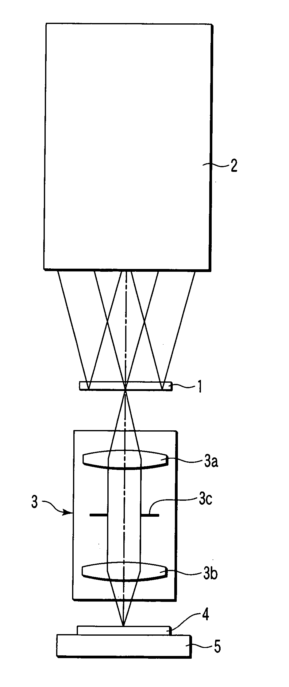
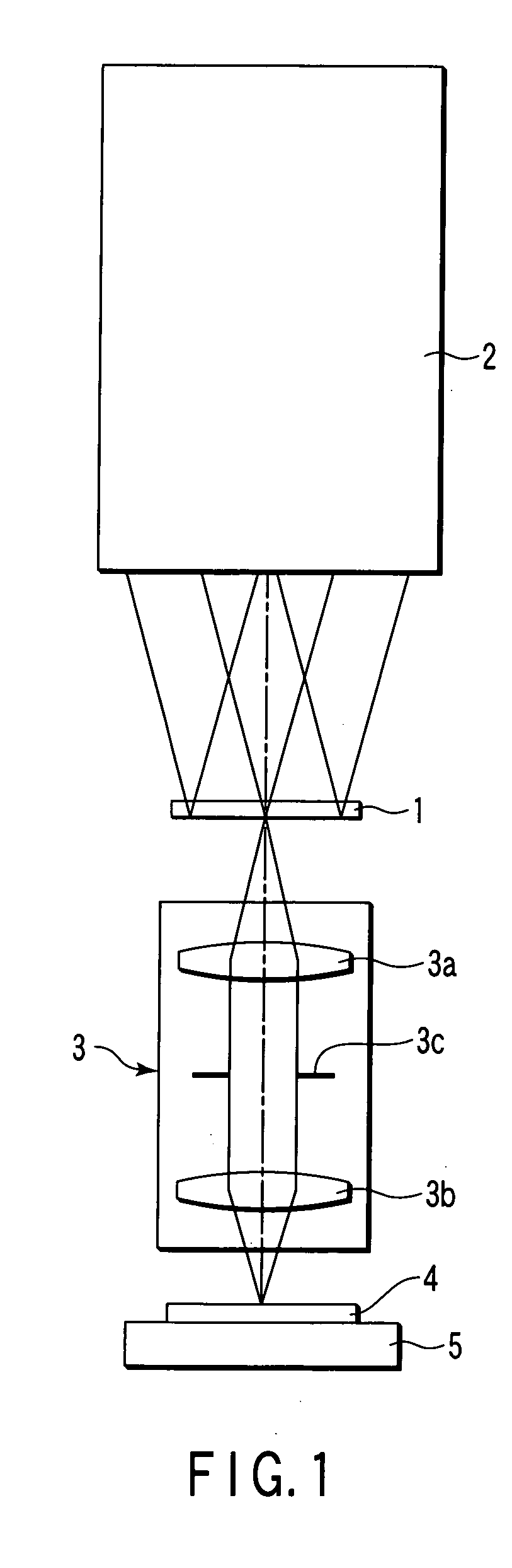
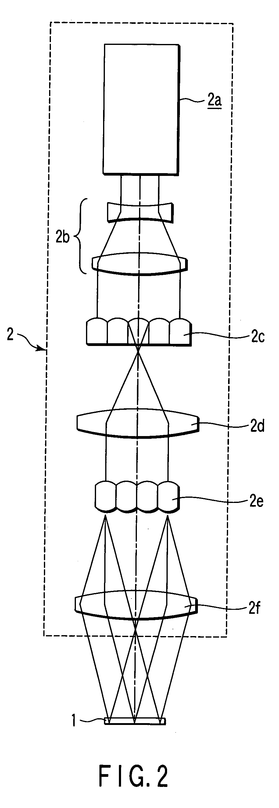
[0050]FIG. 1 is a view schematically showing a structure of a crystallization apparatus according to an embodiment of the present invention. Moreover, FIG. 2 is a view schematically showing an internal structure of an illumination system. Referring to FIG. 1, the crystallization apparatus according to this embodiment includes a light modulation element 1 which modulates a phase of an incident light beam, an illumination system 2, an image formation optical system 3, and a substrate stage 5. A processed substrate (a support substrate such as a glass substrate and a non-single-crystal semiconductor film directly or indirectly formed thereon) 4 is mounted on the stage 5. The detailed substructure and the effects of the light modulation element 1 will be described later.

[0051] As shown in FIG. 2, the illumination system 2 includes a light source 2a which outputs an...


PUM

PropertyMeasurementUnit
Angleaaaaaaaaaa
Angleaaaaaaaaaa
Ratioaaaaaaaaaa

Abstract

A light irradiation apparatus includes a light modulation element which modulates a phase of an incident light beam to obtain a V-shaped light intensity distribution having a bottom portion of a minimum light intensity, and an image formation optical system which applies the modulated light beam from the light modulation element to an irradiation target surface in such a manner that the V-shaped light intensity distribution is provided on the irradiation target surface. The light modulation element has such a complex amplitude transmittance distribution that a secondary derivative of a phase value of a complex amplitude distribution becomes substantially zero at the bottom portion of the V-shaped light intensity distribution in an image space of the image formation optical system.

Description

CROSS-REFERENCE TO RELATED APPLICATIONS [0001] This application is based upon and claims the benefit of priority from prior Japanese Patent Application No. 2004-039747, filed Feb. 17, 2004, the entire contents of which are incorporated herein by reference. BACKGROUND OF THE INVENTION [0002] 1. Field of the Invention [0003] The present invention relates to a light irradiation apparatus, a light irradiation method, a crystallization apparatus, a crystallization method, a device, and a light modulation element. [0004] 2. Description of the Related Art [0005] A thin film transistor (TFT) which is used for a switching element or the like which selects a display pixel in, e.g., a liquid crystal display (LCD) has been conventionally formed in an amorphous silicon layer or a polysilicon layer. [0006] The polysilicon layer has a higher mobility of electrons or holes than the amorphous silicon layer. Therefore, when a transistor is formed in a polysilicon layer, a switching speed is increased...

Claims


Application Information

Patent Timeline
IPC IPC(8): B23K26/00B23K26/06B23K26/073B23K26/08G02F1/00G02F1/133G03B27/54G03F7/20H01L21/00H01L21/20H01L21/324H01L21/77
CPCB23K26/0656B23K26/073H01L27/1296H01L21/2026H01L27/1285B23K26/08B23K26/066H01L21/02686H01L21/02488H01L21/02422H01L21/02598H01L21/02502H01L21/02678H01L21/02532A61F13/84A61F13/42G01N33/493G01N33/50A61F2013/422A61F2013/8473A61F2013/8488
Inventor TANIGUCHI, YUKIO
Owner SHARP KK
Why Eureka
Try Eureka