Self testing CMOS imager chip

a self-testing, imager chip technology, applied in the field of photosensitive imagers, can solve the problems of insufficient monitoring of imager operation, insufficient detection of in-field failures or changes in imager performance, so as to reduce the noise of fixed pattern, eliminate the need for expensive light injection and measurement test equipment, and enhance the operation of the imager

Active Publication Date: 2005-08-25
DELPHI TECH IP LTD
View PDF1 Cites 13 Cited by
  • Summary
  • Abstract
  • Description
  • Claims
  • Application Information

AI Technical Summary

Benefits of technology

[0004] Each pixel includes a collect gate, a read gate, and a dump gate. The collect gate, when enabled, collects charge due to the incident light. This charge is transferred to the read gate, and to the control electronics by energizing the gates according to a predetermined sequence referred to as the read cycle. After the control electronics read the image charge of the pixel, the dump gate is energized to move the charge to a sewer, thereby erasing the image charge. The sewer is defined as a heavily doped implantation or diffusion region connected to the pixel, which is normally used to drain off charge from the pixel after the readout sequence. In this application, this region is also used as a source of charge to be injected into the pixel without using a light source. The pixel is read again in the absence of light to measure the background charge, and the background charge is compared by the control electronics to the image charge according to a conventional...

Problems solved by technology

Such test equipment is generally quite sophisticated and correspondingly expensive.
Additionally, operational testing at the manufacturer, while benefici...

Method used


Image

  • Self testing CMOS imager chip
  • Self testing CMOS imager chip
  • Self testing CMOS imager chip

Examples


Embodiment Construction

[0012] The embodiments of the invention described herein are not intended to be exhaustive or to limit the invention to the precise forms disclosed. Rather, the embodiments selected for description have been chosen to enable one skilled in the art to practice the invention.

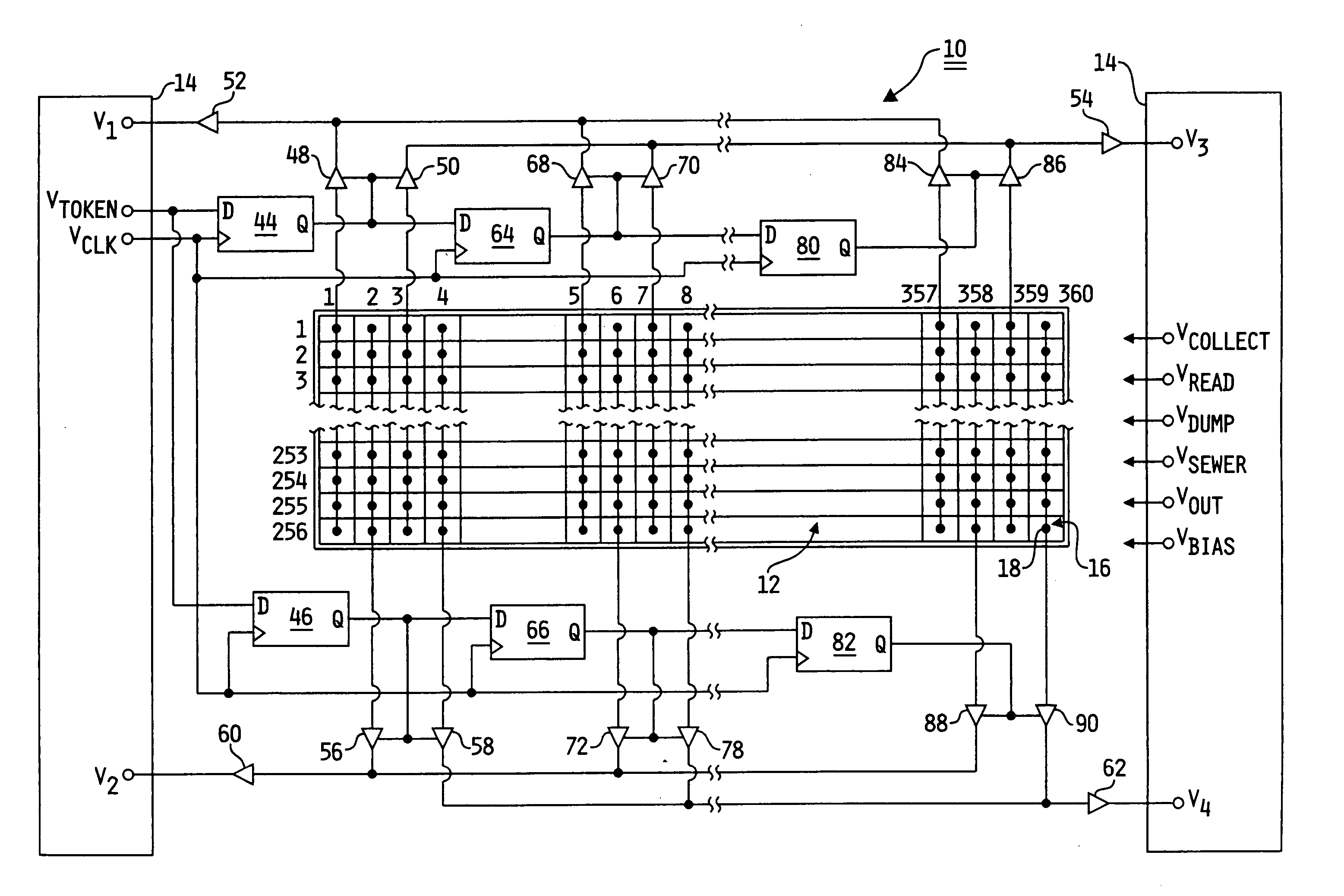
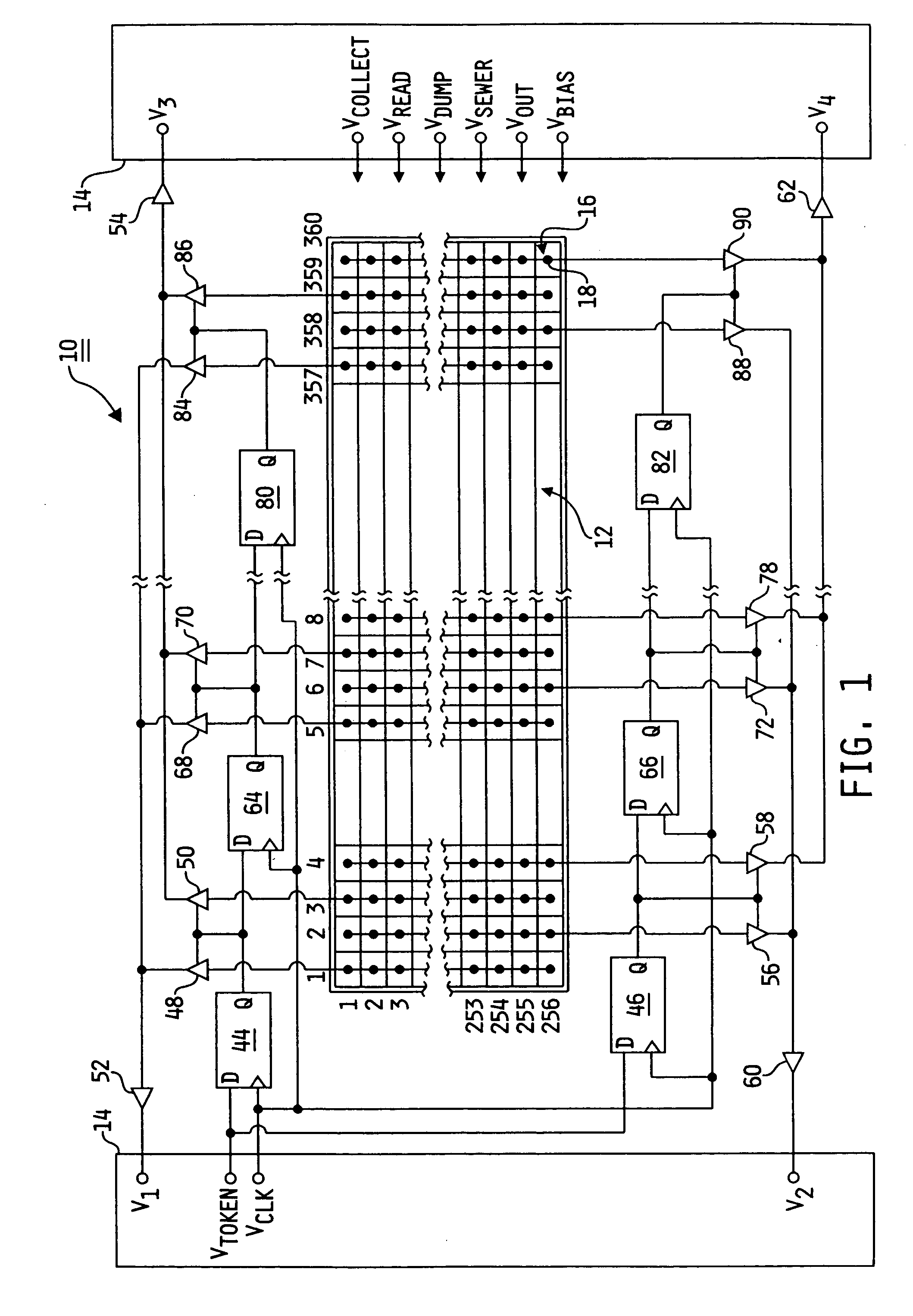
[0013] Referring now to FIG. 1, imager 10 generally includes a pixel array 12, a controller 14 for inputting control signals to pixel array 12 and receiving output signals from the read-out electronics (the remaining electronics shown in FIG. 1). Pixel array 12 is arranged in 226 rows of 360 pixels 16 each. Each pixel 16 includes an output node 18. As shown in FIG. 1, the output nodes 18 of pixels 16 in each of the 360 columns are connected together and to the read-out electronics as will be further described below. It should be understood that the size of array 12 (i.e., the number of rows and columns) is irrelevant in terms of implementing the teachings of the present invention.

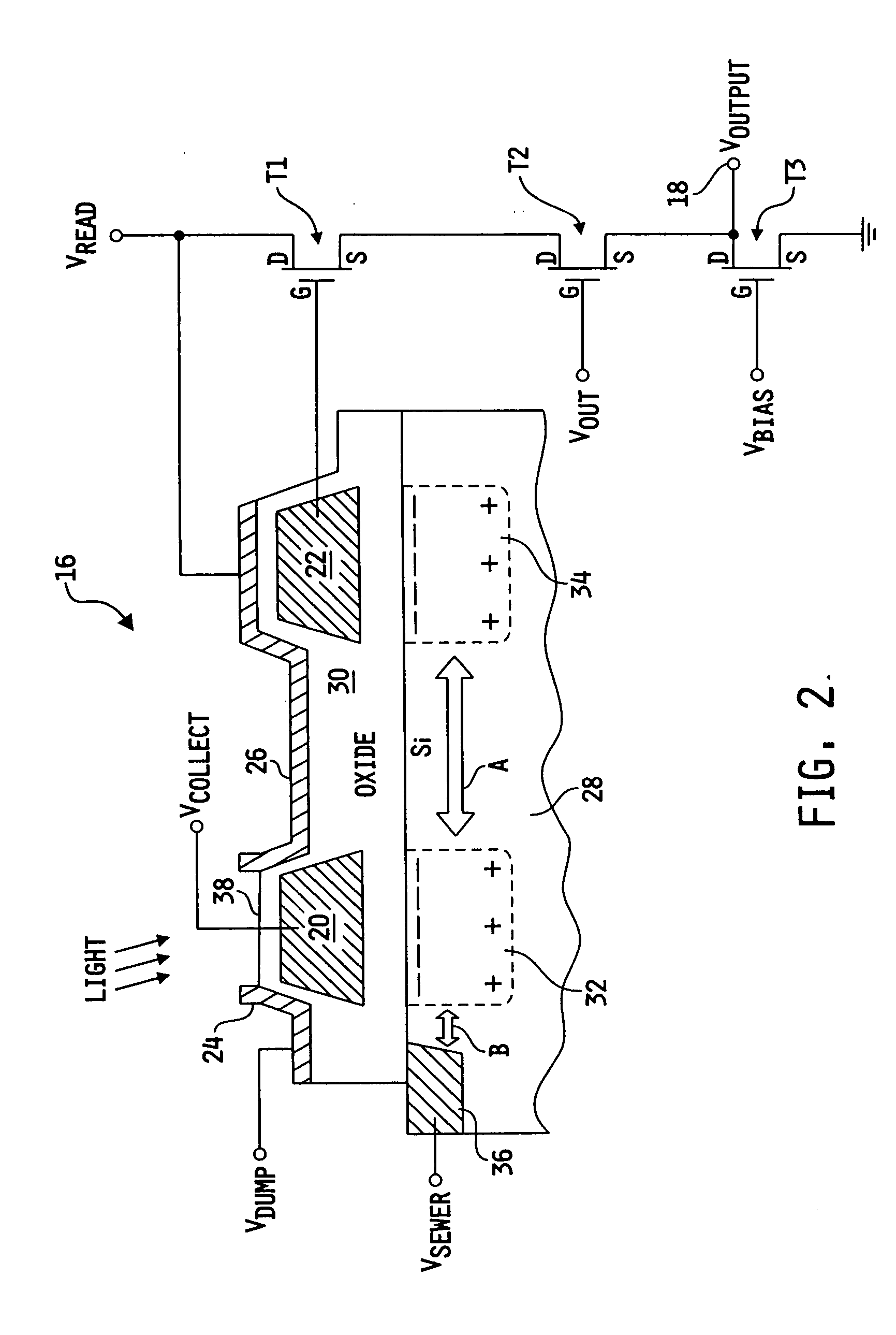
[0014]FIG. 2 is a cross-sectiona...


PUM


Abstract

A self testing CMOS imager chip includes a controller which outputs a sewer signal, a dump signal, a collect signal, and a read signal, and a pixel array connected to the controller including a plurality of pixels arranged in an array of rows and columns, each pixel having a collect gate disposed adjacent a collect well for receiving a charge in response to application of the collect signal to the collect gate, a sewer for injecting a charge into the collect well in response to the concurrent application of the sewer signal to the sewer and the collect signal to the collect well, a read gate disposed adjacent a read well for receiving the injected charge from the collect well in response to application of the read signal to the read gate and the absence of the collect signal at the collect gate, and a transistor having a gate coupled to the read well, a source for receiving the read signal, and a drain coupled to an output node connected to the controller. The read signal is modulated by the injected charge at the gate of the transistor, thereby generating an injected output signal at the output node representing the injected charge. The controller, through read-out circuitry, comparing the injected output signal to an expected output signal to test the operation of each pixel of the array.

Description

TECHNICAL FIELD [0001] The present invention relates generally to photo-sensitive imagers, and more particularly, to a photo-capacitive imager chip with an electrical charge injection feature for self testing the imager chip. BACKGROUND OF THE INVENTION [0002] Photo-sensitive imagers collect charge due to incident light to sense the presence or absence of objects which affect the amount of incident light available to the imager. In the automotive industry, for example, imagers are used as sensors in lane tracking systems, edge-of-road detection systems, near-obstacle-avoidance detection systems, crash alert systems and passenger position sensing systems. Such safety critical applications require imagers with high reliability. Accordingly, conventional imagers, which are typically photo-diode imagers, are tested at the manufacturer using precision equipment to inject a known quantity of light and compare the imager output to the expected output resulting from the known quantity of li...

Claims


Application Information

Patent Timeline
IPC IPC(8): H01L27/00H01L27/146H01L31/00H04N5/365H04N5/374H04N5/378
CPCH01L27/14643H04N17/002H04N5/374H04N25/76
Inventor SCHAUERTE, FRANK J.MURRAY, BRIAN T.TROXELL, JOHN R.STEVENSON, CHARLES N.
Owner DELPHI TECH IP LTD
Why Eureka
Try Eureka