Method for manufacturing crystal plate
a manufacturing method and crystal plate technology, applied in the direction of polycrystalline material growth, crystal growth process, after-treatment details, etc., can solve the problems of overlapping processing expense, high average damage in the process, and high futility
- Summary
- Abstract
- Description
- Claims
- Application Information
AI Technical Summary
Benefits of technology
Problems solved by technology
Method used
Image
Examples
Embodiment Construction
[0029] Preferred embodiments of the present invention are described in more detail below with reference to the accompanying drawings.
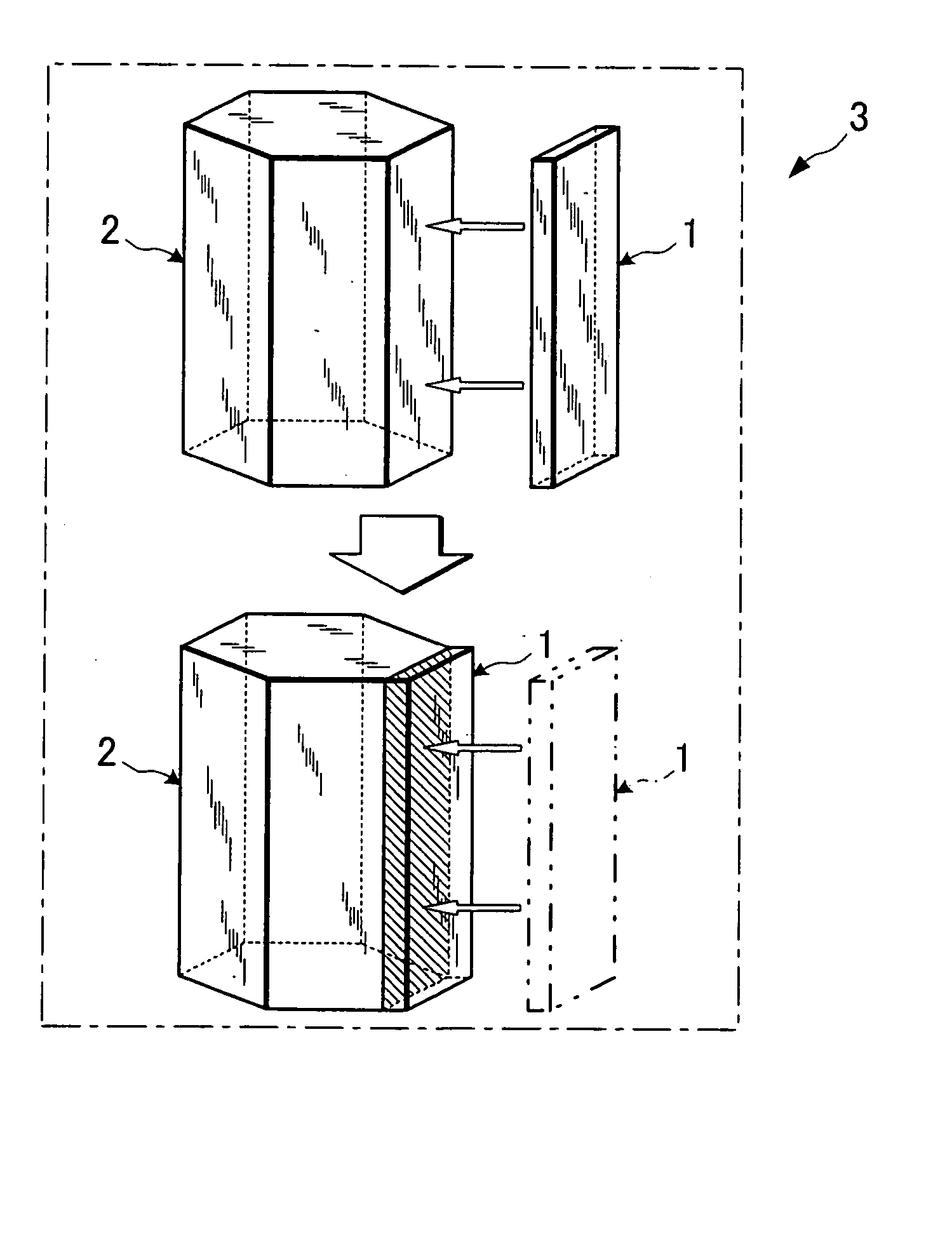
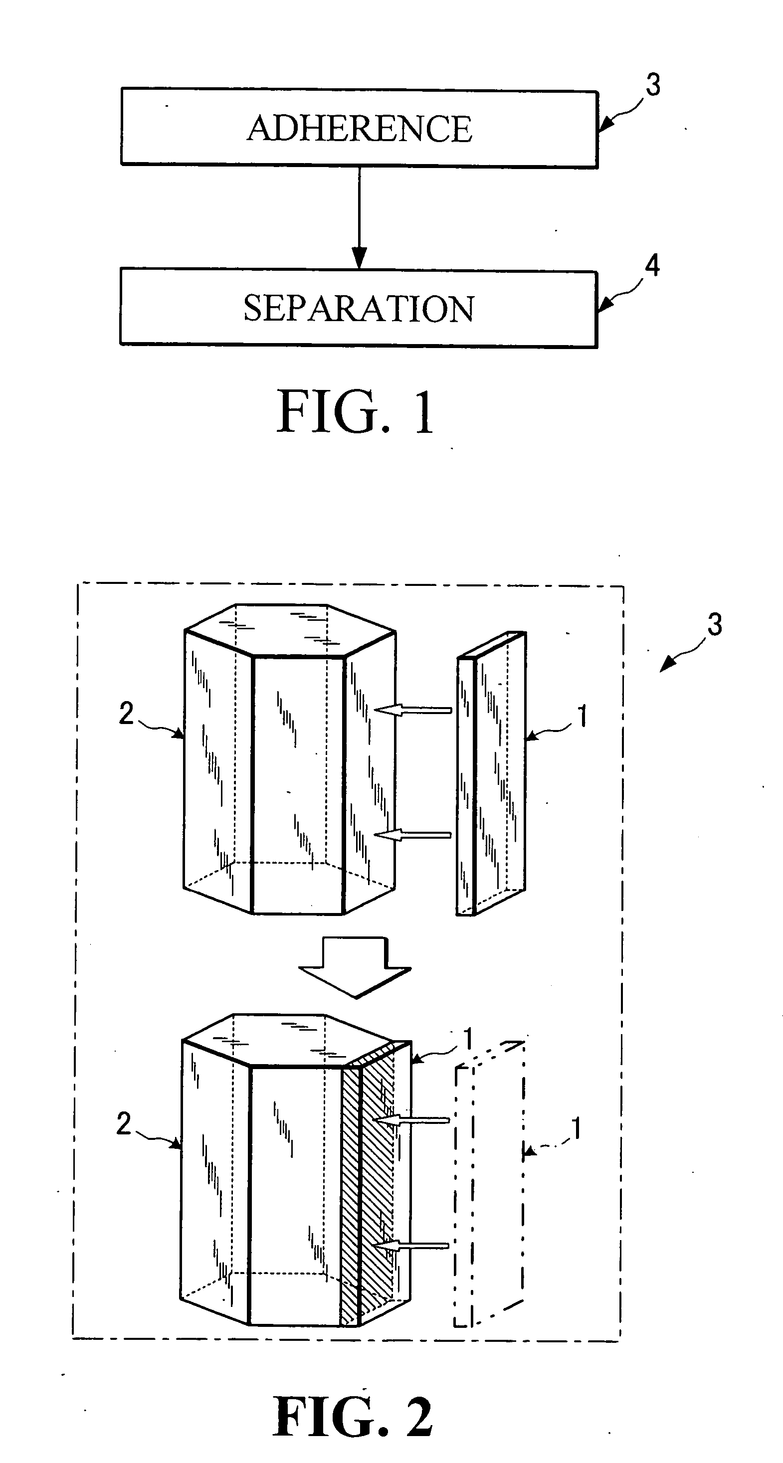
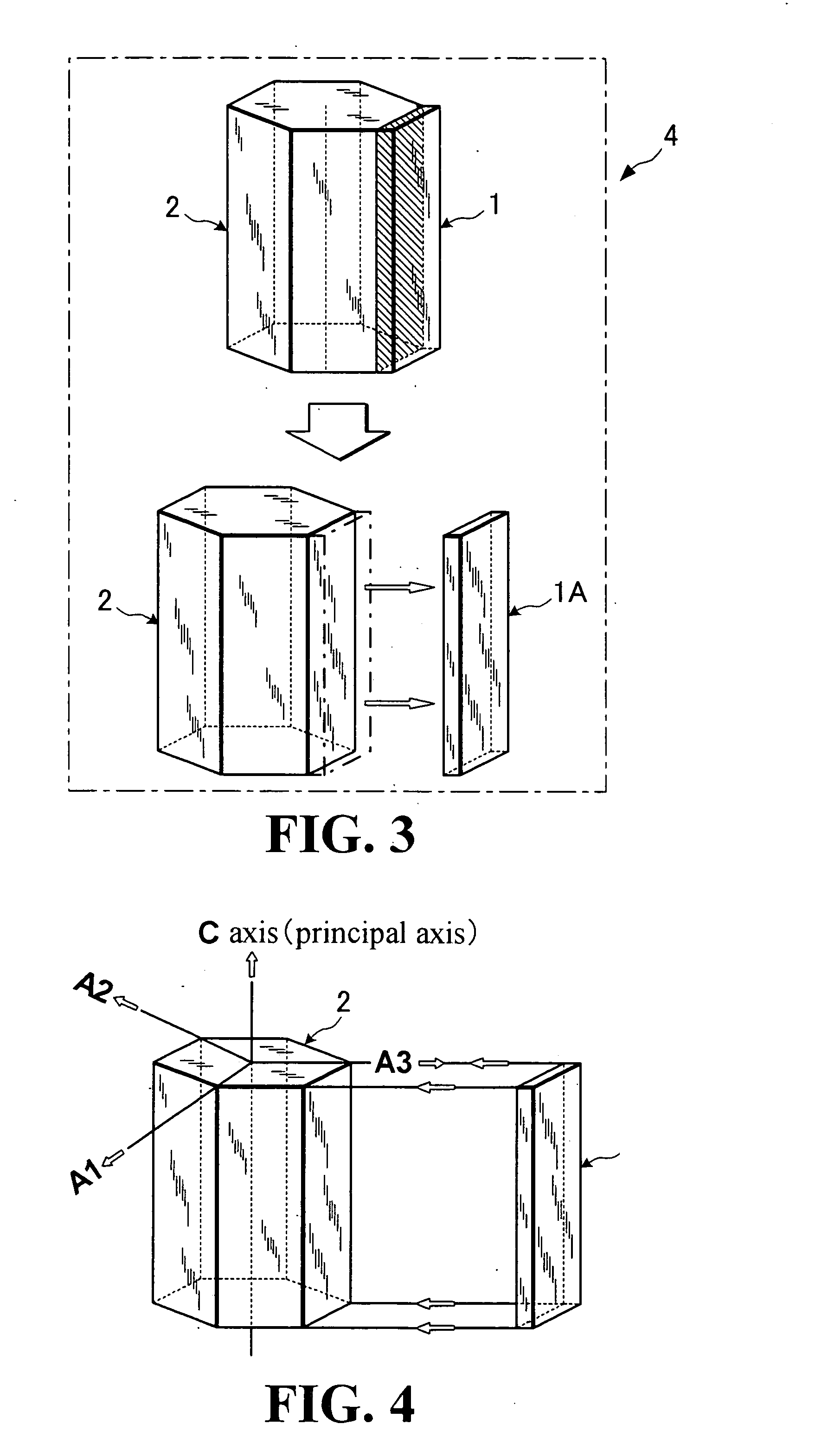
[0030]FIGS. 1-6 illustrate a method for manufacturing a crystal plate in accordance with a first embodiment of the present invention. The manufacturing method includes a step 3 for adhering an amorphous plate 1 and a crystalline body 2 integrally or merging with the amorphous plate 1 and the crystalline body 2; and a step 4 for separating the amorphous plate 1 from the crystalline body 2 after the crystal structure of the crystalline body 2 is copied to the amorphous plate 1.
[0031] By this method, after the amorphous plate 1 without the crystal structure is induced the crystalline body 2 with the crystal structure and separates, the amorphous plate 1 is set to a crystal plate 1A with the same crystal structure as the crystalline body 2. Here, in this case of the embodiment, the crystal structure chooses and assumes a hexagonal system crystal having A...
PUM
 Abstract
Description
Claims
Application Information


