TFT, flat panel display device having the same, method of manufacturing TFT, method of manufacturing flat panel display device, and method of manufacturing donor sheet

a flat panel display device and transistor technology, applied in the field of thin film transistors, can solve the problems of difficult to acquire flexible flat panel display devices, reducing electrical characteristics and reliability, and unable to easily increase the region of display devices

Inactive Publication Date: 2005-09-01
SAMSUNG DISPLAY CO LTD
View PDF3 Cites 64 Cited by
  • Summary
  • Abstract
  • Description
  • Claims
  • Application Information

AI Technical Summary

Benefits of technology

[0013] It is therefore an object of the present invention to provide an improved design for a flat panel display.

Problems solved by technology

However, when the semiconductor active layer is formed of amorphous silicon, electrical characteristics and reliability are lowered, and the region of a display device cannot be easily increased.
However, when a TFT is formed of polycrystalline silicon using a conventional method, it is difficult to acquire a flexible flat panel display device.
These plastic materials have low heat resistance, and if present when polycrystalline is formed, these materials will not tolerate heat well.

Method used


Image

  • TFT, flat panel display device having the same, method of manufacturing TFT, method of manufacturing flat panel display device, and method of manufacturing donor sheet
  • TFT, flat panel display device having the same, method of manufacturing TFT, method of manufacturing flat panel display device, and method of manufacturing donor sheet
  • TFT, flat panel display device having the same, method of manufacturing TFT, method of manufacturing flat panel display device, and method of manufacturing donor sheet

Examples


Embodiment Construction

[0036] As a preliminary matter, as used herein, the term (TMS)2Se means bis(trimethylsillyl)selenium; the term TOPSe means (Tri-n-octylphosphine)selenide, and the term TBPSe means (Tributylphosphine)selenide.

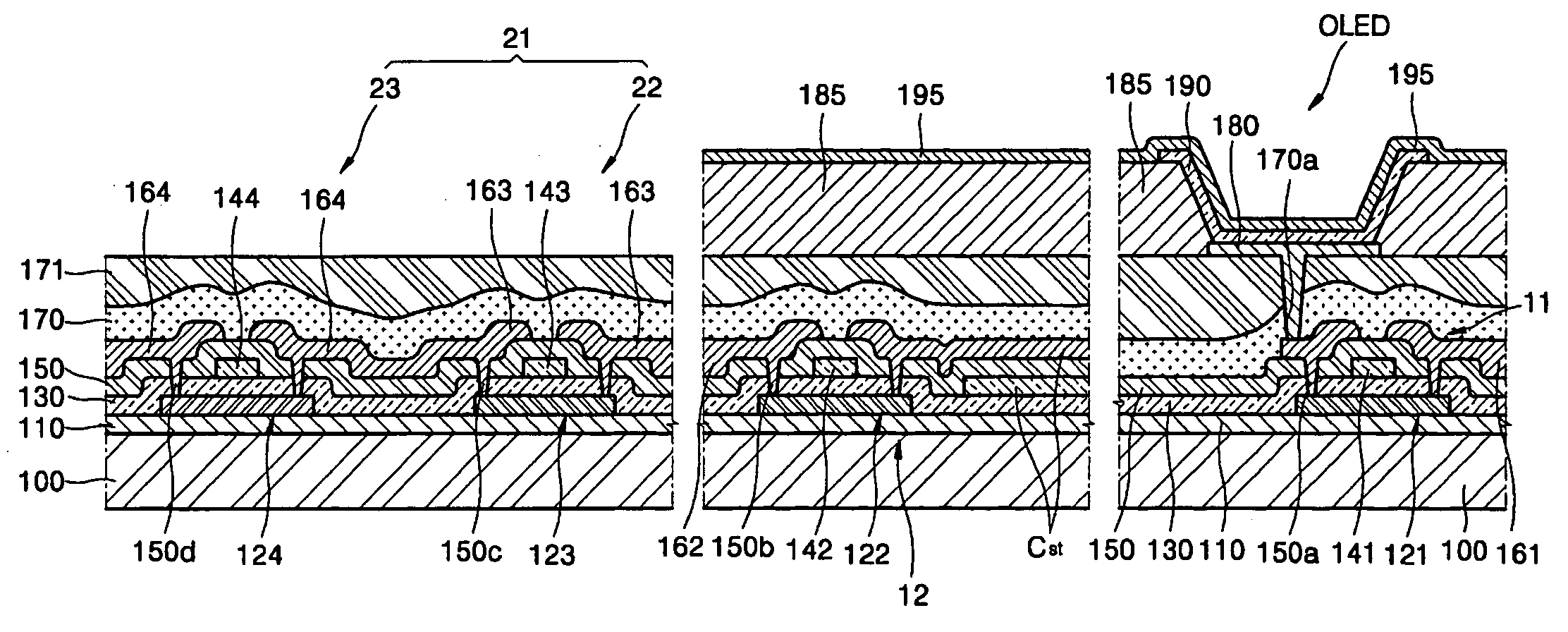
[0037] Turning now to the figures, FIG. 1 is a schematic diagram of an emission region 10 and a non-emission region 20 of an (OLED) flat panel display 1. A plurality of subpixels where an OLED and a selection driving circuit are disposed, are located in the emission region 10 of display 1. A horizontal driver (HD) and / or a vertical driver (VD) for driving the subpixels is located in the non-emission region 20. FIG. 1 shows only the VD within the non-emission region 20, but a plurality of circuits such as the HD or a level shifter may be located in the non-emission region 20. In addition, a terminal portion connected to an external circuit and a sealing portion for sealing the emission region 10 etc. are located in the non-emission region 20.

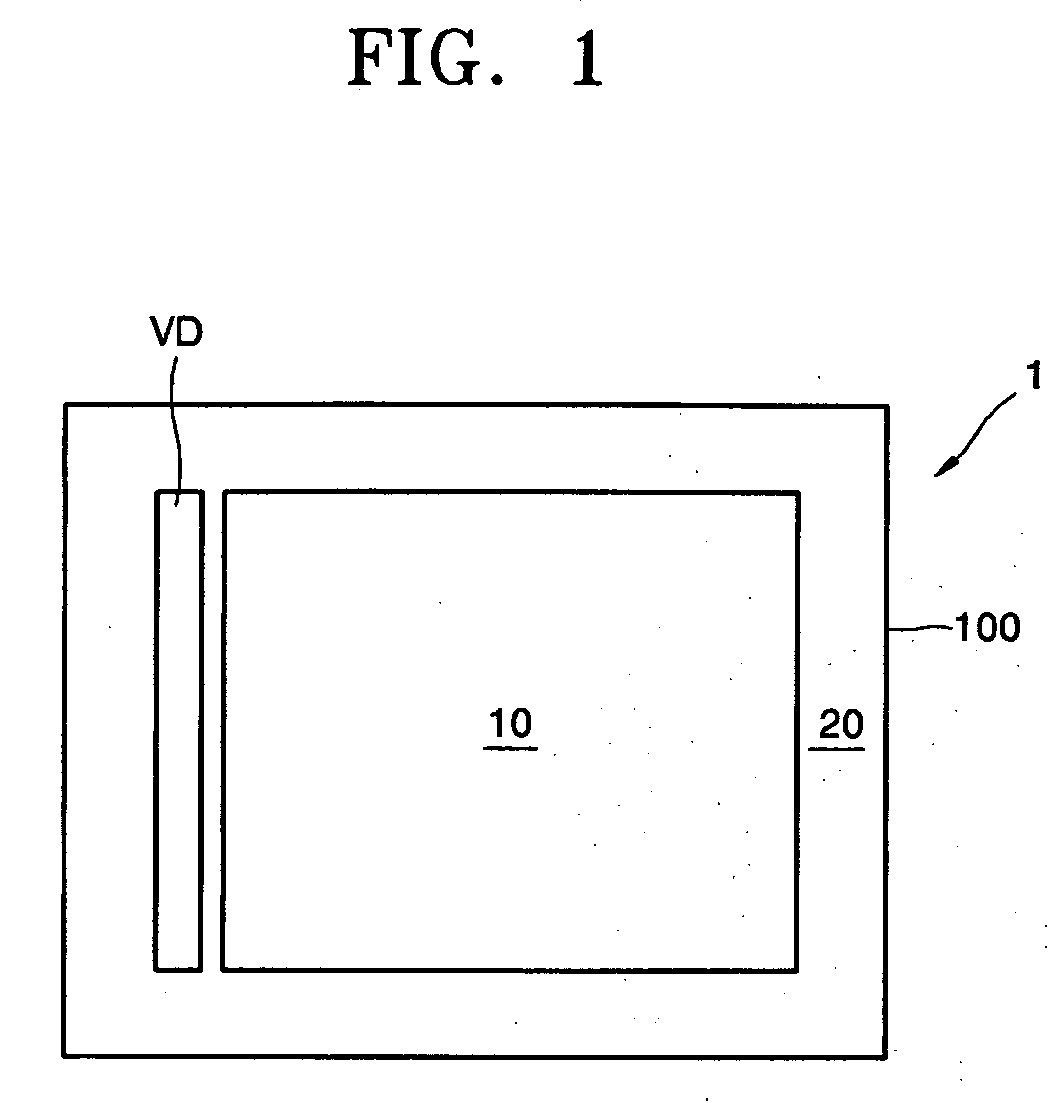
[0038] Turning now to FIG. 2, FIG. 2...


PUM

PropertyMeasurementUnit
temperatureaaaaaaaaaa
widthaaaaaaaaaa
thicknessaaaaaaaaaa

Abstract

A flexible flat panel display where nanoparticles are used for the active layer of the TFTs and the substrate is flexible and can be manufactured at room temperature, a flat panel display device having the same, a method of manufacturing a TFT, a method of manufacturing a flat panel display device, and a method of manufacturing a donor sheet. In making the TFTs in the display, a donor sheet is used to transfer the nanoparticles from the sheet to the substrate. The thin film transistor is placed on a substrate and includes a channel region which has at least one P-type or N-type nanoparticle arranged in a lengthwise direction, wherein the lengthwise direction of the P-type or N-type nanoparticles is parallel to a P-type or an N-type nanoparticle line partitioned off on the substrate.

Description

CLAIM OF PRIORITY [0001] This application makes reference to, incorporates the same herein, and claims all benefits accruing under 35 U.S.C. §119 from applications earlier filed in the Korean Intellectual Property Office on 26 Feb. 2004 and 19 Apr. 2004 and there duly assigned Serial Nos. 2004-13007 and 2004-26648, respectively. BACKGROUND OF THE INVENTION [0002] 1. Field of the Invention [0003] The present invention relates to a thin film transistor (TFT), a flat panel display device having the same, a method of manufacturing a TFT, a method of manufacturing a flexible flat panel display device, and a method of manufacturing a donor sheet, and more particularly, to a TFT using nanoparticles in at least a channel, a flat panel display device having the same, a method of manufacturing a TFT, a method of manufacturing a flat panel display device, and a method of manufacturing a donor sheet. [0004] 2. Description of the Related Art [0005] A flat panel display device such as a liquid cr...

Claims


Application Information

Patent Timeline
Patent Type & Authority Applications(United States)
IPC IPC(8): B82B1/00H05B33/00G02F1/136G09F9/30G09G3/10G09G3/36H01L21/336H01L27/32H01L29/04H01L29/06H01L29/786H01L51/00H01L51/50H05B33/10H05B33/12H05B33/14
CPCB82Y20/00B82Y30/00H01L27/3244H01L29/04H01L29/786H01L29/78681H01L29/66969H01L29/7869H01L51/0013H01L51/0097H01L2251/5338H01L2251/5369H01L29/78684H10K59/12H10K71/18H10K77/111H10K2102/311H10K2102/331F24F6/14F24F13/20F24F13/28
Inventor SUH, MIN-CHULYANG, NAM-CHOULKOO, JAE-BONKIM, HYE-DONGCHUNG, HO-KYOONLEE, UL-HO
Owner SAMSUNG DISPLAY CO LTD
Why Eureka
Try Eureka