
Sine wave multiplication circuit and sine wave multiplication method

a multiplication circuit and sine wave technology, applied in the field of sine wave multiplication circuit and sine wave multiplication method, can solve the problems of 40 db, considerably difficult to ensure 40 db, and cannot anticipate the high degree of accuracy of arithmetic operation, so as to reduce the feed-through and the effect of an image componen

Inactive Publication Date: 2005-09-08
SONY CORP
View PDF5 Cites 3 Cited by
  • Summary
  • Abstract
  • Description
  • Claims
  • Application Information

AI Technical Summary

Benefits of technology

[0009] It is an object of the present invention to provide a sine wave multiplication circuit and a sine wave multiplication method which can achieve reduction of the feed-through and an image component.

Problems solved by technology

However, a high degree of accuracy in arithmetic operation cannot be anticipated with such an analog multiplier as described above.
The most serious problem is an offset.
Even though, it is considerably difficult to assure −40 dB.

Method used


Image

  • Sine wave multiplication circuit and sine wave multiplication method
  • Sine wave multiplication circuit and sine wave multiplication method
  • Sine wave multiplication circuit and sine wave multiplication method

Examples


example 1

CIRCUIT EXAMPLE 1

[0058] Now, particular circuit examples of the weighting circuit 10 and the polarity changeover circuit 13 are described. FIG. 14 shows a circuit example (circuit example 1) which has two addition coefficients and operates with k=4, that is, eight-time sampling.

[0059] Various methods are applicable to implement the weighting circuit 10 and the polarity changeover circuit 13. In FIG. 14, a circuit example which uses an operational amplifier OP having differential inputs / outputs is shown. Where the weighting circuit 10 and the polarity changeover circuit 13 are implemented using differential inputs / outputs in this manner, they can be implemented very simply. In particular, the weighting circuit 10 and the polarity changeover circuit 13 can be formed from a resistor network 21 including resistors R1 and R2 and a switch circuit 22 including switches SWm, SWp and SWpx. The switch SWm is used to change over the weighting coefficient, and the switches SWp and SWpx are use...

example 2

CIRCUIT EXAMPLE 2

[0062]FIG. 16 shows a particular circuit example (circuit example 2) of the weighting circuit 10 and the polarity changeover circuit 13 where k=8, that is, for 16-time sampling. FIG. 17 illustrates control of switches and weighting coefficients in the case of the circuit example 2. Switches SWp and SWpx for changing over the polarity are same as those in the circuit example 1. In the present circuit example, three different types of switches SWma, SWmb and SWmcx are used in order to change over the weighting coefficient among four different weighting coefficients.

[0063] When to provide a maximum weighting coefficient m1, the switches SWma and SWmb are on and the switch SWmcx is off. If the switches SWma are turned off in this state, then the weighting coefficient m2 is provided, and if the switches SWmb are turned off further, then the weighting coefficient m3 is provided. If the switch SWmcx is turned on further, then the minimum weighting coefficient m4 is provid...

example 3

CIRCUIT EXAMPLE 3

[0066]FIG. 18 shows a circuit example (circuit example 3) implemented by a buffer circuit equivalently having an input switch function.

[0067] Referring to FIG. 18, the sine wave multiplication circuit according to the circuit example 3 includes a buffer amplifier 23 having two inputs to which potentials as nodes N1 and N2 of a resistor network 21A formed from three resistors connected in series between an input in+ to the sine wave multiplication circuit and the ground. The sine wave multiplication circuit further includes another buffer amplifier 24 having two inputs to which potentials at nodes N3 and N4 of another resistor network 21B formed from three resistors connected in series between the other input in− to the sine wave multiplication circuit and the ground. The sine wave multiplication circuit further includes a further buffer amplifier 25 having two inputs to which outputs of the buffer amplifiers 23 and 24 are inputted, and a still further buffer amplif...


PUM


Abstract

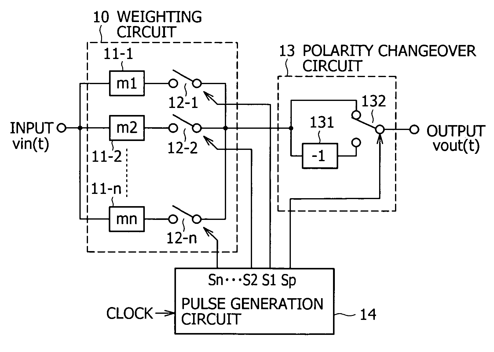
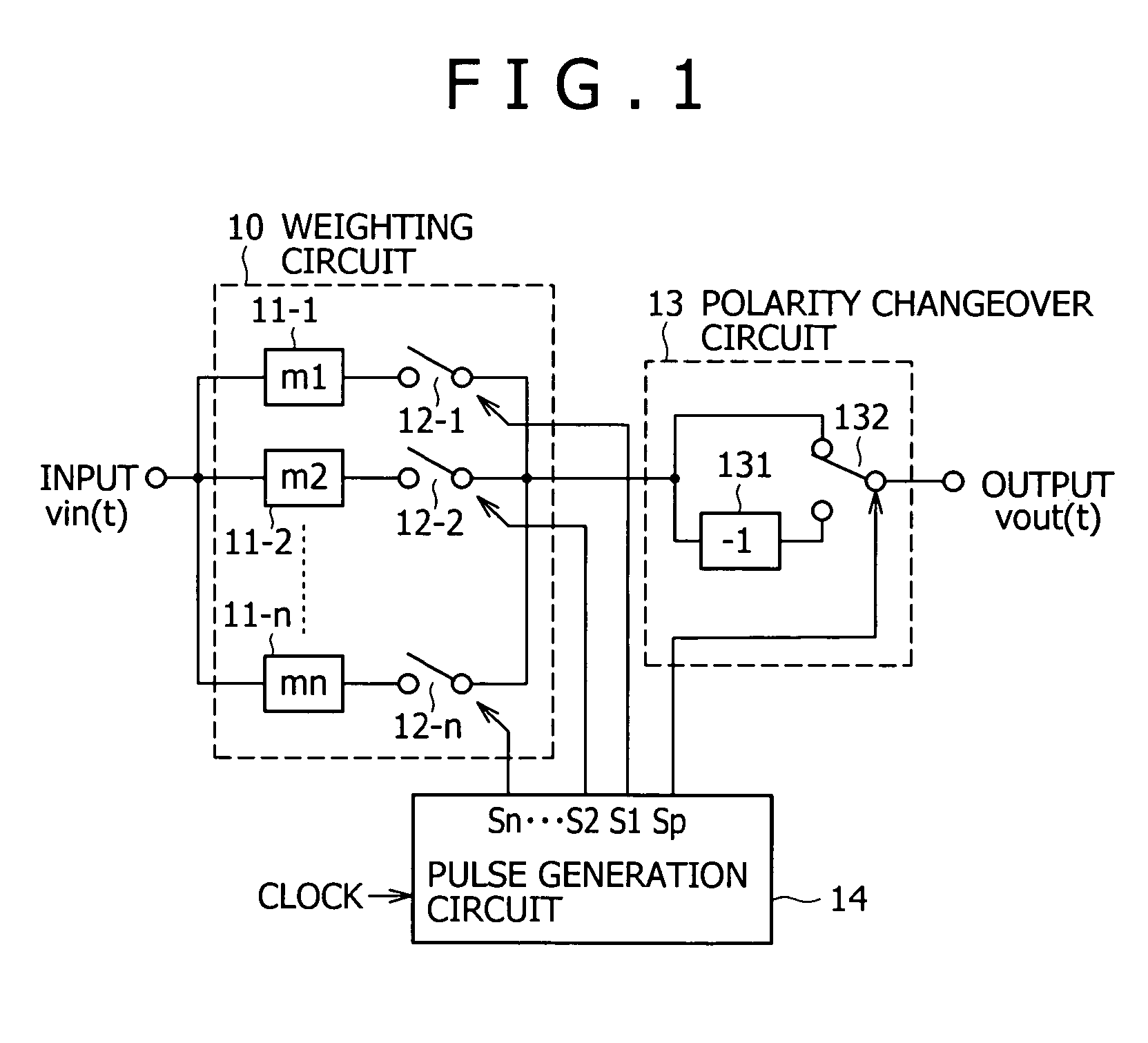
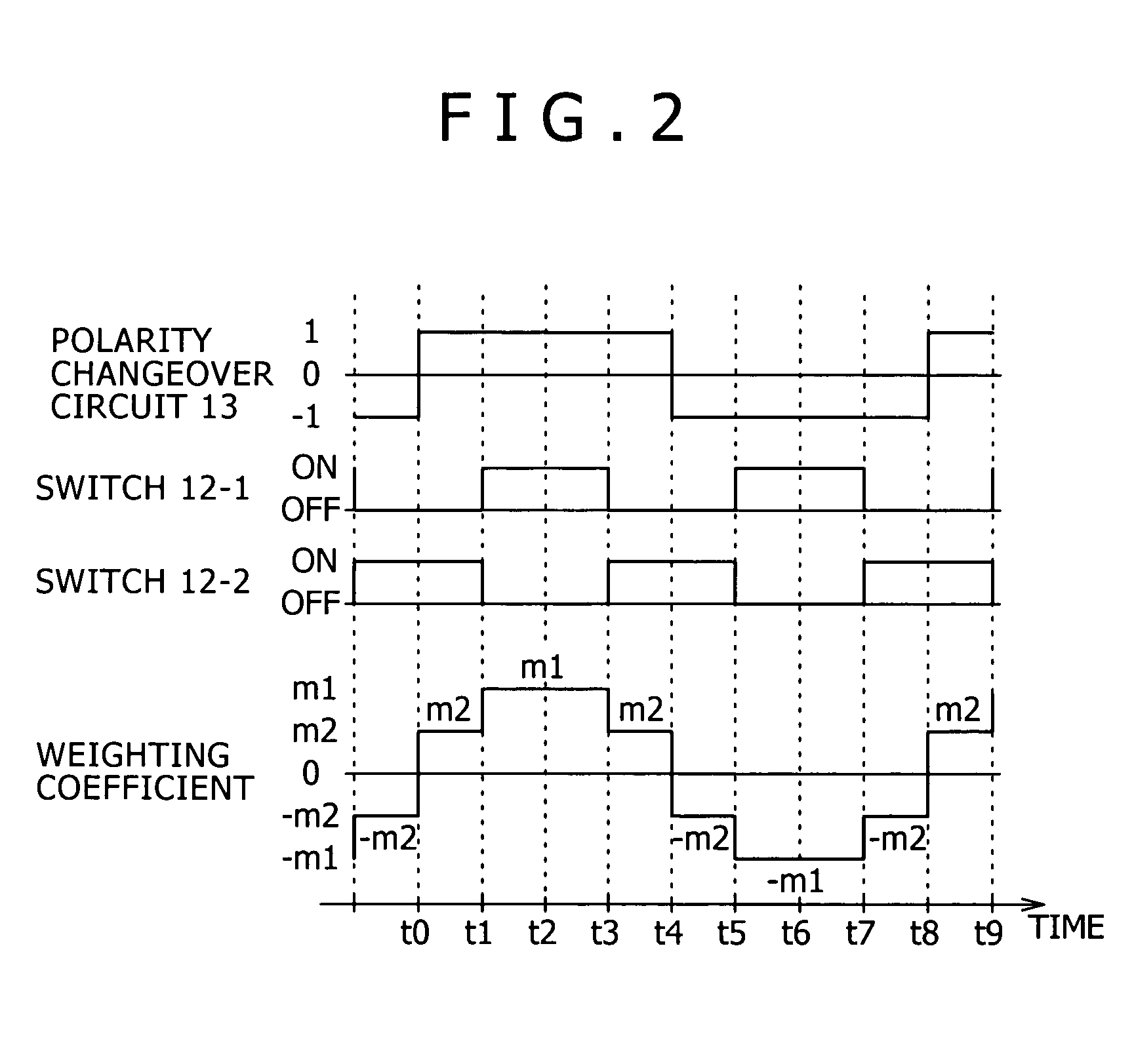
A sine wave multiplication circuit multiplies an analog input signal by n (n is an integer equal to or greater than 2) weighting coefficients each having a unique value. The polarity of the analog input signal multiplied by one of the n weighting coefficients is changed over. Further, changeover among the n weighting coefficients and of the polarity is performed after every sampling period equal to ½k (k is an integer, and 2k is equal to or greater than 6 but equal to or smaller than 4n) of one period of the sine wave signal by which the analog input signal is multiplied. As a result, a staircase waveform having 2n positive and negative stairs is generated while unnecessary harmonic wave components in the proximity of the sine wave signal by which the analog input signal is multiplied can be reduced.

Description

BACKGROUND OF THE INVENTION [0001] This invention relates to a sine wave multiplication circuit and a sine wave multiplication method for multiplying a certain analog signal by a sine wave signal, and more particularly to an analog sine wave multiplication circuit and an analog sine wave multiplication method for a sine wave signal. [0002] It is one of the most basic functions in various signal processes to multiply a certain signal by a sine wave. For example, in frequency conversion of shifting a certain signal by a desired frequency, a sine wave multiplication circuit is required. Further, a sine wave multiplication circuit is required essentially also for conversion of a frequency band of a signal into a frequency band in the proximity of zero (direct current) in frequency in order to detect an arbitrary frequency component of the signal. [0003] Here, for example, taking arithmetic operation for determination of an accurate sum of two sine waves as an example, arithmetic operati...

Claims


Application Information

Patent Timeline
Patent Type & Authority Applications(United States)
IPC IPC(8): G06G7/16G06G7/161H03B19/00
CPCH03B19/00G06G7/16H03D7/1466H03D2200/0086H03D7/1458H03D7/1483
Inventor KATAKURA, MASAYUKI
Owner SONY CORP
Learn More