Use of amorphous carbon film as a hardmask in the fabrication of optical waveguides

a technology of optical waveguides and carbon films, applied in glass making apparatus, manufacturing tools, instruments, etc., can solve the problems of affecting the formation of patterned core materials, affecting the propagation of propagation, and affecting the effect of forming patterned core materials

Inactive Publication Date: 2005-09-15
APPLIED MATERIALS INC
View PDF98 Cites 382 Cited by
  • Summary
  • Abstract
  • Description
  • Claims
  • Application Information

AI Technical Summary

Problems solved by technology

If the lower cladding is too thin, the two orthogonal modes see a different effective refractive index resulting in birefringence, a consequential dispersion phenomenon that would limit the width of the transmission window.
However, the use of traditional mask materials to pattern and etch the core material 103, such as photoresist and/or silicon nitride has resulted in difficulties in forming the patterned core materials 103.
Further, photoresist material and silicon nitride have had difficulties in being removed from the core material without forming defects in the core material, ...

Method used


Image

  • Use of amorphous carbon film as a hardmask in the fabrication of optical waveguides
  • Use of amorphous carbon film as a hardmask in the fabrication of optical waveguides
  • Use of amorphous carbon film as a hardmask in the fabrication of optical waveguides

Examples


Embodiment Construction

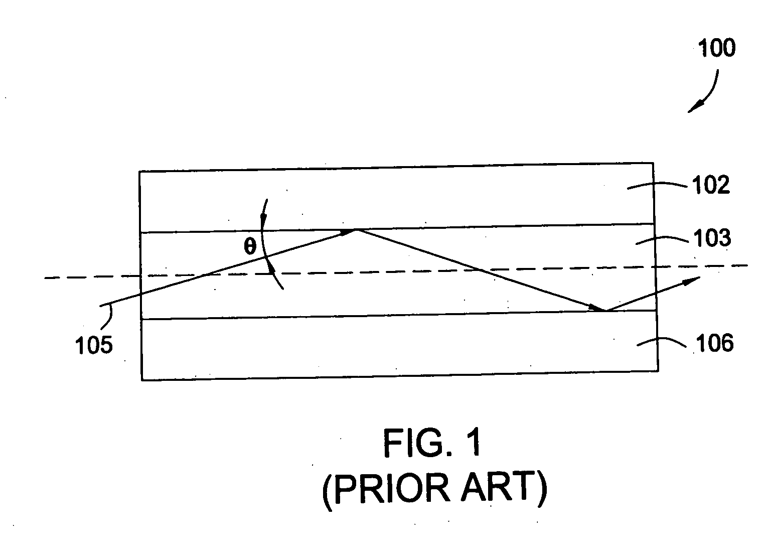
[0017] Aspects of the invention generally provide methods for depositing, processing and removing amorphous carbon material disposed on a core material with minimal or reduced defect formation in forming optical devices, such as waveguides. The words and phrases used herein should be given their ordinary and customary meaning in the art by one skilled in the art unless otherwise further defined.

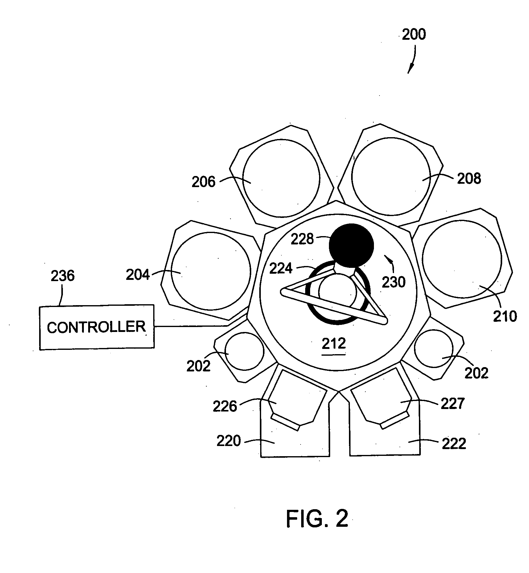
[0018]FIG. 2 is a schematic partial view of one embodiment of a conventional cluster tool, or integrated system, for executing processing steps described herein. An integrated system is desirable to perform a sequence of processing steps while maintaining the substrate in a vacuum environment to reduce contamination and increase throughput. It is contemplated to execute certain processing steps of the novel technique in a cluster tool, similar to, for example, the cluster tool known as the Centura® system manufactured by Applied Materials, Inc. of Santa Clara, Calif.

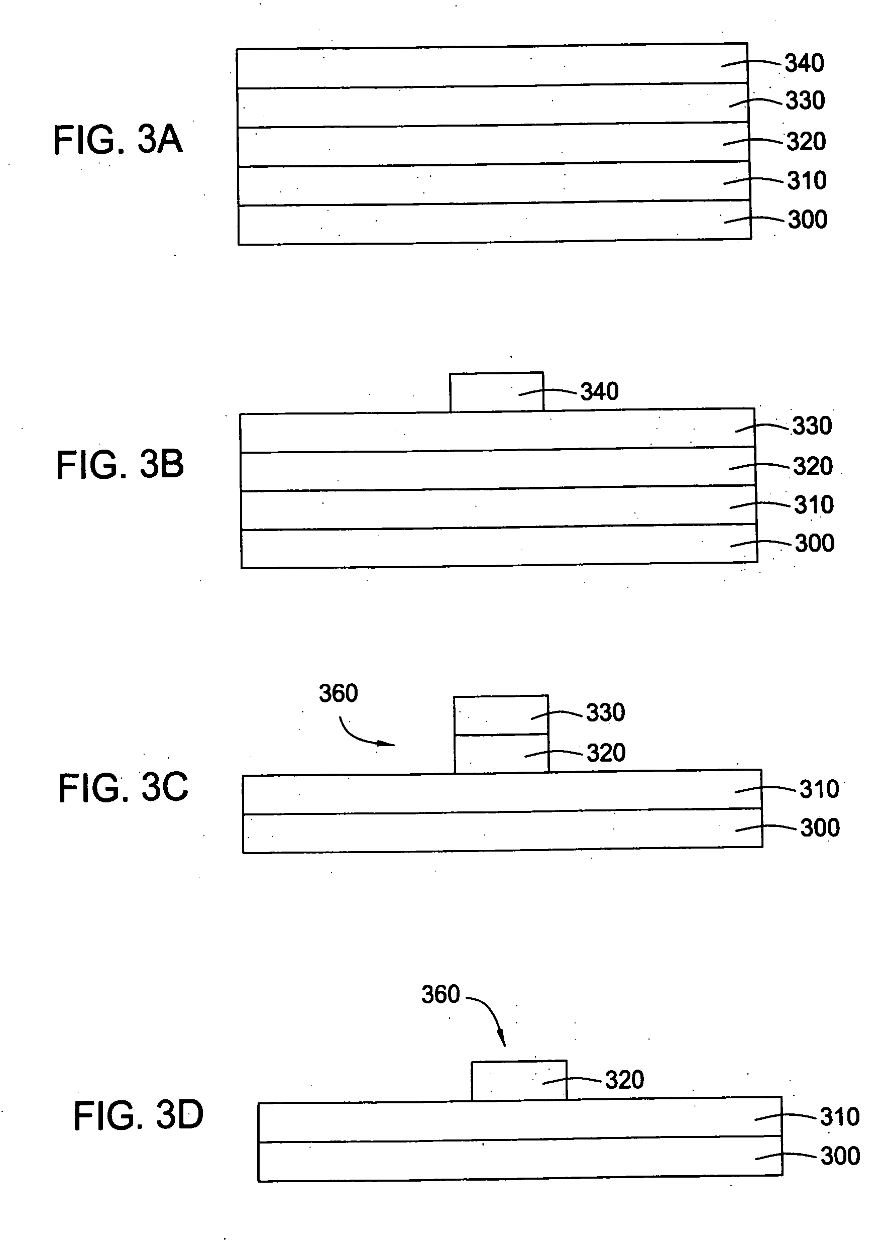
[0019] As schematically ...


PUM

PropertyMeasurementUnit
Compositionaaaaaaaaaa
Selectivityaaaaaaaaaa
Refractive indexaaaaaaaaaa

Abstract

Methods are provided for forming optical devices, such as waveguides, with minimal defect formation. In one aspect, the invention provides a method for forming a waveguide structure on a substrate surface including forming a cladding layer on the substrate surface, forming a core layer on the cladding layer, depositing an amorphous carbon hardmask on the core layer, forming a patterned photoresist layer on the amorphous carbon hardmask, etching the amorphous carbon hardmask, and etching the core material.

Description

BACKGROUND OF THE INVENTION [0001] 1. Field of the Invention [0002] Embodiments of the present invention generally relate to methods and apparatus for fabricating optical devices, such as optical integrated circuits (ICs). [0003] 2. Description of the Related Art [0004] Optical systems are emerging technologies that offer solutions to many previously unsolvable technological problems. Thus, optical systems are now gaining an ever increasing importance in the technology world of today. Generally, optical systems utilize pulses of light rather than electric current to carry out such functions as data transmission, data routing, or other forms of data communication or data processing. One important structure commonly utilized in optical systems is an optical waveguide. [0005] Optical waveguides are used to confine and direct light between the various components of an optical system. For example, optical waveguides may be used to carry Dense Wavelength Division Multiplexed (DWDM) light,...

Claims


Application Information

Patent Timeline
IPC IPC(8): C03B37/018
CPCC03B19/143C03B19/1469C03B2201/31C03B2201/24C03B2201/28C03B2201/10Y02P40/57
Inventor VANDROUX, LAURENTMONCHOIX, HERVE
Owner APPLIED MATERIALS INC
Why Eureka
Try Eureka