Sensor device

a sensor and circuit chip technology, applied in the direction of acceleration measurement using interia force, film/foil adhesives without carriers, vehicular safety arrangments, etc., can solve the problems of circuit chip malfunction, lower side of sensor chip damage to circuit chip, and decrease in performan

Inactive Publication Date: 2005-09-15
DENSO CORP
View PDF4 Cites 2 Cited by
  • Summary
  • Abstract
  • Description
  • Claims
  • Application Information

AI Technical Summary

Benefits of technology

[0009] In view of the above-described problems, it is an object of the present invention to provide a sensor device having a sensor chi...

Problems solved by technology

As a result, the lower side of the sensor chip damages the circuit chip by pressing the lumps in the filler against the surface of the circuit chip when the sensor...

Method used


Image

  • Sensor device
  • Sensor device

Examples


Embodiment Construction

[0022] The following is a description of an embodiment of the present invention with reference to the drawings.

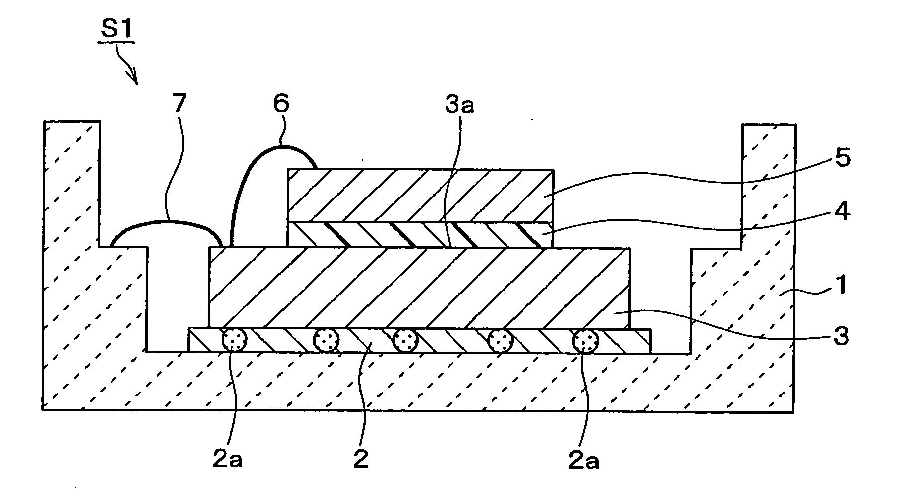
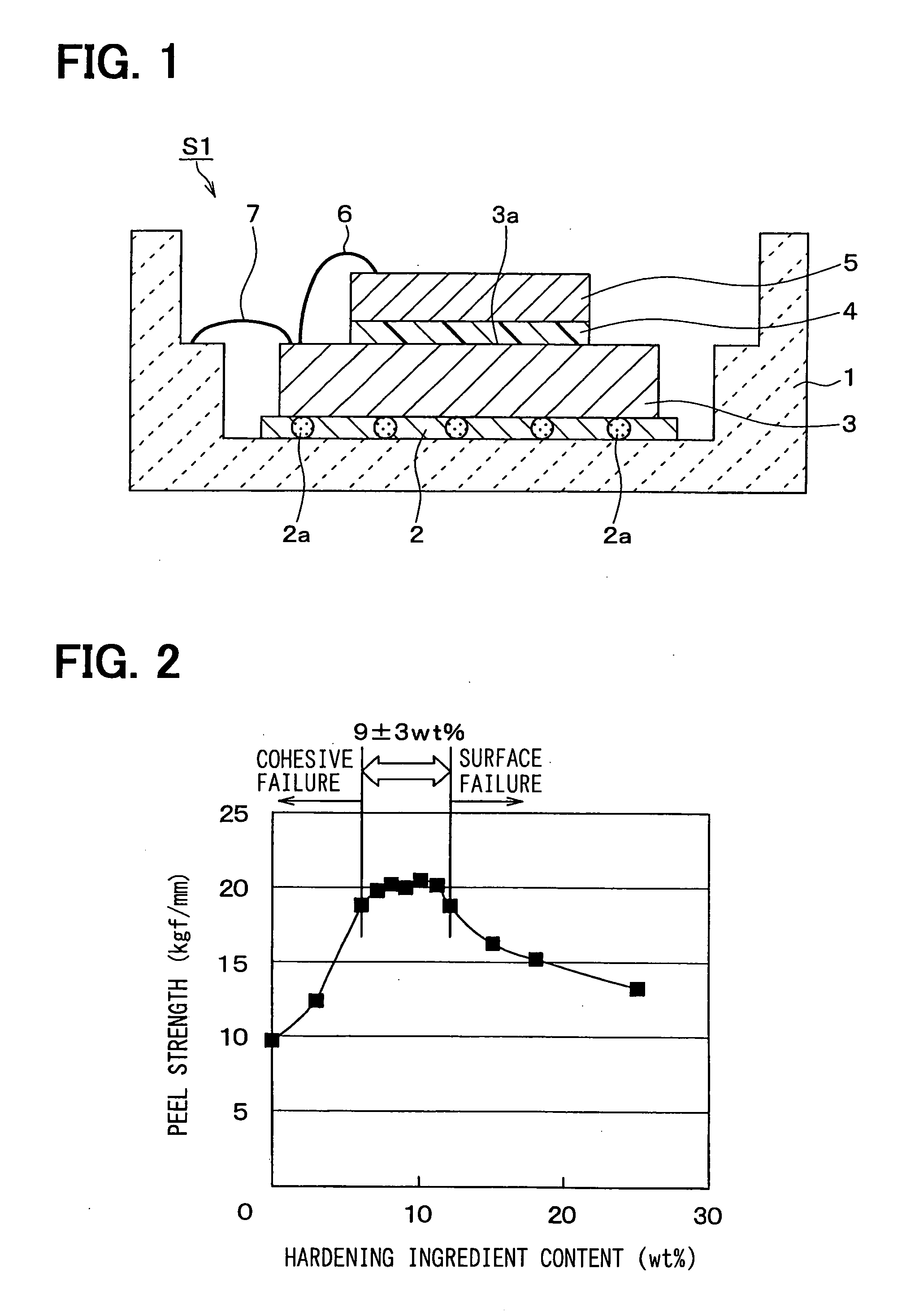
[0023] A sensor device used as an acceleration sensor S1 is shown in FIG. 1 in cross-sectional view. The acceleration sensor S1 is, for example, used for an automotive air-bag device.

[0024] A ceramic package 1 is used as a base of the acceleration sensor S1 as well as an attachment used for attaching the sensor S1 at a suitable place for measurement (e.g. at a bottom of a driver's seat of a vehicle). The accelerator sensor S1 includes a circuit chip 3 disposed on the ceramic package 1. A liquid adhesive 2 made of a silicon-type resin is interposed between the ceramic package 1 and the circuit chip 3.

[0025] In this embodiment, the adhesive 2 contains beads 2a made of resin or the like. The beads 2a serve to establish the thickness of the adhesive 2 in order to level the upper surface of the circuit chip 3 relative to the ceramic package 1. In other words, the beads 2a act...


PUM

PropertyMeasurementUnit
Percent by massaaaaaaaaaa
Thicknessaaaaaaaaaa

Abstract

A sensor device includes a circuit chip and a sensor chip. The circuit chip has a bonding portion. The sensor chip is stacked on the bonding portion of the circuit chip. The circuit chip and the sensor chip are bonded by a film-type adhesive containing 91 ±3 weight % of polyimide with no filler.

Description

CROSS REFERENCE TO RELATED APPLICATIONS [0001] This application is based on Japanese Patent Application No. 2004-69025 filed on Mar. 11, 2004 and Japanese Patent Application No. 2004-309615 filed on Oct. 25, 2004, the disclosures of which are incorporated herein by reference. FIELD OF THE INVENTION [0002] The present invention relates to a sensor device having a sensor chip, a circuit chip, and a film-type adhesive interposed therebetween. BACKGROUND OF THE INVENTION [0003] A conventional sensor device such as an acceleration sensor and / or an angular speed sensor includes a circuit chip with a bonding portion, a sensor chip stacked on the bonding portion of the circuit chip, and a film-type adhesive interposed between the circuit chip and the sensor chip. [0004] In this type of conventional sensor device, a stack structure that mounts the sensor chip on top of the circuit chip is adopted in order to reduce manufacturing costs by minimizing an implementation size. [0005] The adhesive...

Claims


Application Information

Patent Timeline
IPC IPC(8): G01P15/08B60R21/01C09J5/04C09J7/10G01P15/00G01P15/125H01L21/50H01L23/18H01L25/065H01L31/00
CPCB81B2207/012B81C3/001H01L2224/73265H01L2224/73257H01L2224/73204H01L2224/48145H01L2224/48091H01L2224/32225H01L2224/32145C09J7/00C09J179/08C09J2203/326C09J2479/08G01P1/023G01P15/0802H01L23/293H01L2924/13091H01L2924/1305H01L2224/16225H01L2924/00014H01L2924/00C09J7/10C08K7/00C08K2201/005C09J2301/408H01L2924/00012B07B1/4609
Inventor IKEZAWA, TOSHIYATANAKA, MASAAKI
Owner DENSO CORP
Why Eureka
Try Eureka