Light emission display, display panel, and driving method thereof

Active Publication Date: 2005-09-15
SAMSUNG DISPLAY CO LTD
View PDF5 Cites 192 Cited by
  • Summary
  • Abstract
  • Description
  • Claims
  • Application Information

AI Technical Summary

Benefits of technology

[0020] In one embodiment of the present invention, a pixel circuit is provided. The pixel circuit is coupled to a first scan line for applying a first signal, a second scan line for applying a second signal, and a data line for applying a data voltage and includes: a driving transistor, a display element, a first switching transistor, a compensation device, a storage capacitor, and a second switching transistor. The driving transistor includes a control electrode, a first electrode coupled to a first power source, and a second electrode and is for outputting a current corresponding to a voltage between the first electrode and the control electrode. The di

Problems solved by technology

Also, a short range (SR) uniformity problem is generated because the amount of currents supplied to the organic EL element OLED is varied by a deviation of the threshold voltage (Vth) of a thin

Method used


Image

  • Light emission display, display panel, and driving method thereof
  • Light emission display, display panel, and driving method thereof
  • Light emission display, display panel, and driving method thereof

Examples


Embodiment Construction

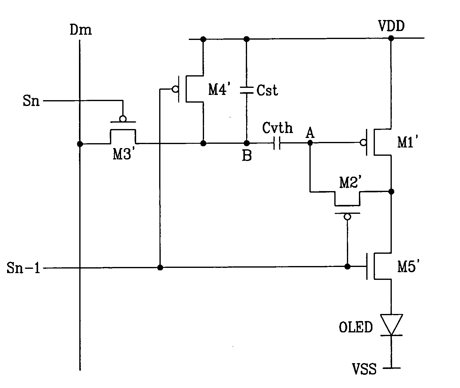
[0032] In the following detailed description, only certain exemplary embodiments of the present invention are shown and described, simply by way of illustration. As those skilled in the art would realize, the described embodiments may be modified in various different ways, all without departing from the spirit or scope of the present invention. Accordingly, the drawings and description are to be regarded as illustrative in nature, and not restrictive. To clarify the present invention, certain components which are not described in the specification can be omitted, and like reference numerals indicate like components.

[0033]FIG. 5 shows a brief diagram of a light emission display according to certain exemplary embodiments of the present invention.

[0034] As shown, the light emission display includes an organic EL display panel 100, a scan driver 200, and a data driver 300.

[0035] The organic EL display panel 100 includes a plurality of data lines D1 to Dm arranged in a column directio...


PUM


Abstract

A light emission display includes data lines, scan lines, and pixel circuits. A pixel circuit of the pixel circuits includes: a light emission element; a first transistor including a control electrode and first and second electrodes, the first transistor outputting a current corresponding to a voltage between the first electrode and the control electrode; a first switch coupled between the control electrode of the first transistor and the light emission element and for receiving a first control signal; a first capacitor coupled to the first transistor; a second capacitor coupled between a first power source and the first capacitor; a second switch for coupling the first capacitor and a second power source in response to a second control signal; and a third switch for applying a data voltage to the first capacitor in response to a select signal provided by one of the scan lines.

Description

CROSS REFERENCE TO RELATED APPLICATION [0001] This application claims priority to and the benefit of Korea Patent Application No. 10-2004-0016139 filed on Mar. 10, 2004 in the Korean Intellectual Property Office, the entire content of which is incorporated herein by reference. BACKGROUND OF THE INVENTION [0002] (a) Field of the Invention [0003] The present invention relates to a display device. More specifically, the present invention relates to an organic electroluminescent (EL) display, a display panel, and a driving method thereof. [0004] (b) Description of the Related Art [0005] In general, an organic electroluminescent (EL) display is a display device that electrically excites a phosphorous organic compound in a plurality of organic light emitting diodes (OLEDs) to emit light. The organic EL display voltage- or current-drives N×M organic emitting cells to display images. An organic emitting cell of the organic EL display includes an anode (ITO), an organic thin film, and a cath...

Claims


Application Information

Patent Timeline
IPC IPC(8): G09G3/20H01L51/50G09G3/30G09G3/32H05B44/00
CPCG09G3/3233G09G2300/043G09G2300/0819G09G2320/043G09G2300/0861G09G2310/0262G09G2300/0852B42D5/045B65D5/4266B65D85/54B42P2241/16
Inventor KIM, YANG-WANOH, CHOON-YUL
Owner SAMSUNG DISPLAY CO LTD
Why Eureka
Try Eureka