
Dynamic control of photodiode bias voltage

a photodiode and bias voltage technology, applied in the field of receivers, can solve the problems of reverse bias voltage, receiver noise, damage or destruction of apd, etc., and achieve the effect of cost-effective dynamic control of the photodiode bias voltag

Active Publication Date: 2005-09-22
CIENA
View PDF3 Cites 24 Cited by
  • Summary
  • Abstract
  • Description
  • Claims
  • Application Information

AI Technical Summary

Benefits of technology

[0014] An object of the present invention is to provide methods and apparatus enabling cost effective dynamic control of photodiode bias voltage.
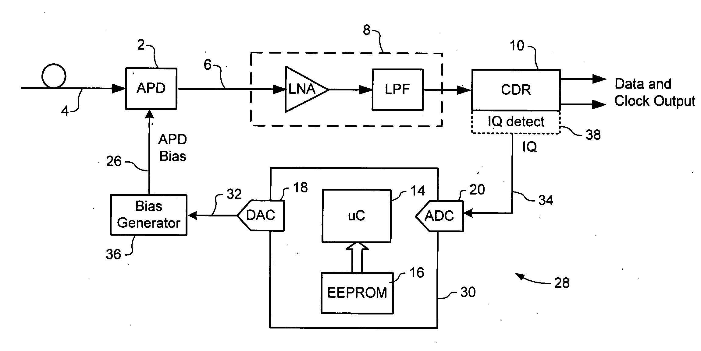
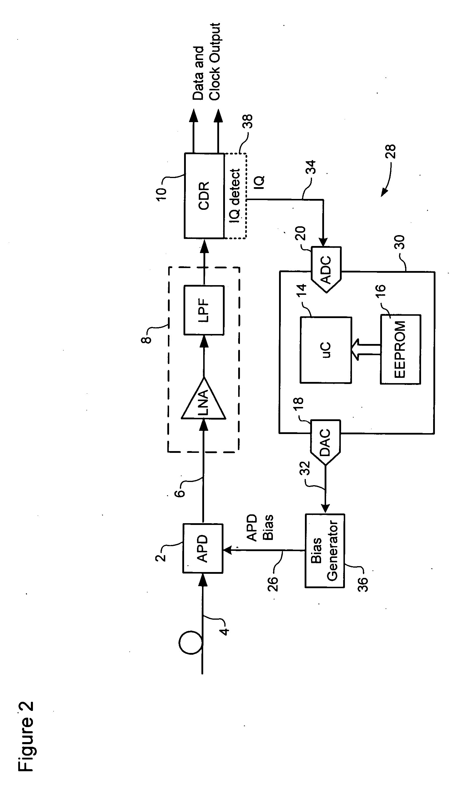
[0015] Accordingly, an aspect of the present invention provides a method of dynamically controlling a bias point of a photodiode of an optical receiver. According to the present invention a performance parameter indicative of an eye opening of an optical signal received by the optical receiver is detected. A bias voltage of the photodiode is dynamically adjusted so as to optimize a value of the detected performance parameter.

Problems solved by technology

For example, when an APD is operated below its reverse breakdown voltage, an increase in the reverse bias voltage results in amplification.
However at a reverse bias voltage equal to the breakdown voltage, dark currents increase exponentially, causing the receiver to be saturated with noise and possibly damaging or destroying the APD.
All of these approaches suffer a limitation in that extensive measurements are required in order to characterize the APD.
These measurements must necessarily be conducted separately for each APD, can be time consuming, and cannot be conducted when the receiver is receiving “live” optical signal traffic.
This also means that updating the characteristic data to compensate for age-related drift of component parameters, for example, may be difficult and / or expensive to implement.
However, this functionality may not succeed in optimizing performance of the receiver as a whole.

Method used


Image

  • Dynamic control of photodiode bias voltage
  • Dynamic control of photodiode bias voltage
  • Dynamic control of photodiode bias voltage

Examples


Embodiment Construction

[0025] The present invention provides a cost effective system for dynamically controlling the bias voltage applied to a photodetector of an optical receiver. In the embodiments described below, the photodetector is an avalanche photodetector (APD) of the type well known in the art. However, the skilled artisan will appreciate that the present invention can equally be used to control the bias point of any other photodetector, such as a PIN diode. Thus, for the purposes of the present application, references to avalanche photodetectors should be understood to also refer to any other type of voltage (or current) biased photodetector elements including, but not limited to PIN diodes.

[0026] In general, the present invention provides a feedback bias control loop which operates to dynamically adjust the bias voltage so as to optimize operation of the optical receiver as a whole. In this respect, receiver optimization implies that the receiver eye quality has been maximized. Thus, the pres...


PUM


Abstract

Accordingly, an aspect of the present invention provides a method of dynamically controlling a bias point of a photodiode of an optical receiver. According to the present invention a performance parameter indicative of an eye opening of an optical signal received by the optical receiver is detected. A bias voltage of the photodiode s dynamically adjusted so as to optimize a value of the detected performance parameter.

Description

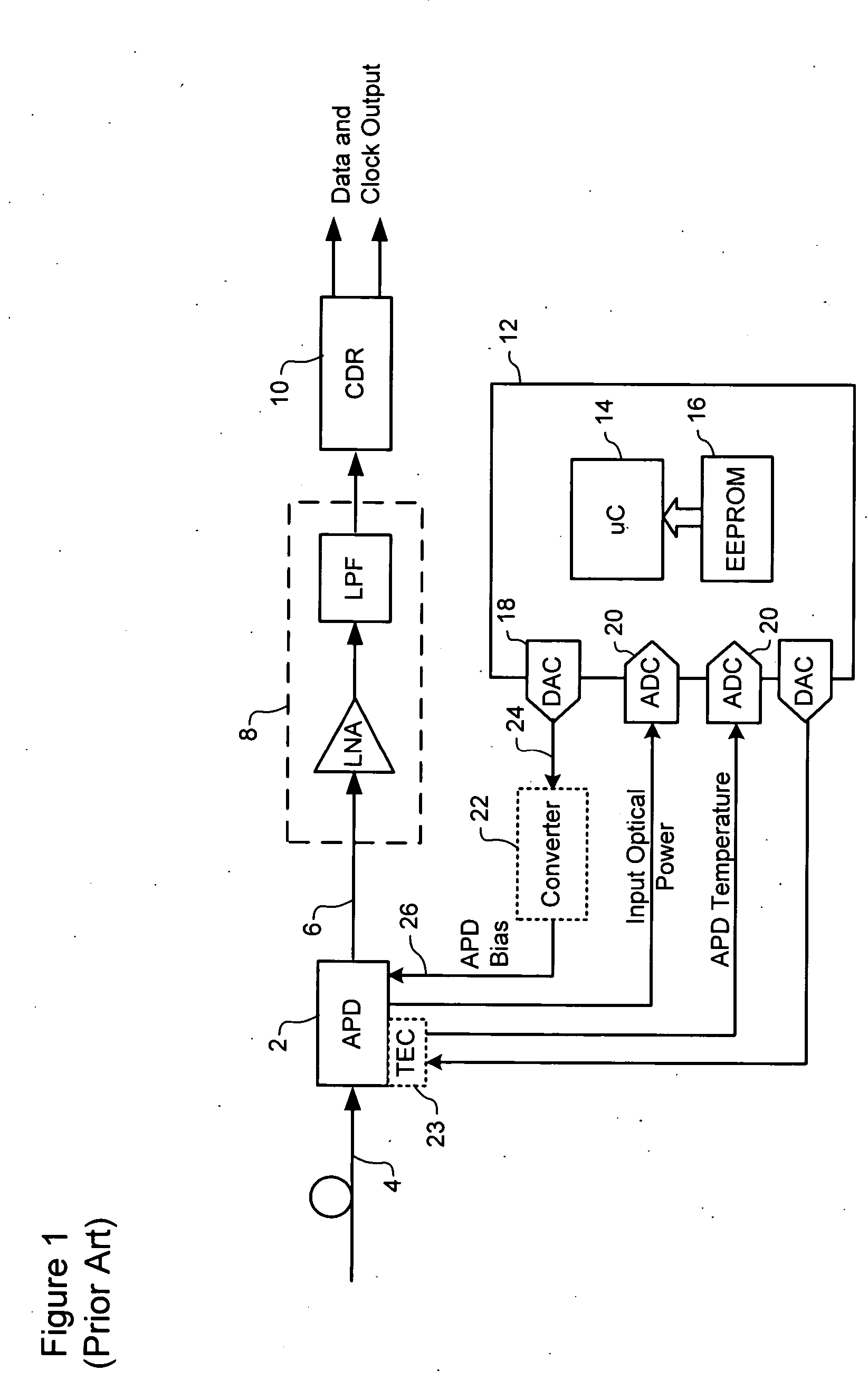
CROSS-REFERENCE TO RELATED APPLICATIONS [0001] This is the first application filed for the present invention. MICROFICHE APPENDIX [0002] Not Applicable. TECHNICAL FIELD [0003] The present invention relates to receivers utilized in optical communication systems, and in particular to methods and systems for dynamically controlling the bias voltage of a photodiode. BACKGROUND OF THE INVENTION [0004] Optical receivers used in communications systems generally comprise a photo-detector 2 for converting an optical signal 4 into an electrical signal 6 (See FIG. 1a). The electrical signal 6 output by the photodetector 2 is supplied to a linear channel 8 that may consist of a high gain amplifier and a low pass filter, and a Clock and Data Recovery (CDR) circuit 10. [0005] The most extensively used photo-detectors in fiber optical systems are the P-Intrinsic-N (PIN) photodiode and the avalanche photodiode (APD). Optical receivers that use an APD normally provide higher sensitivity than that us...

Claims


Application Information

Patent Timeline
Patent Type & Authority Applications(United States)
IPC IPC(8): H01L31/00H01L31/02H04B10/158
CPCH04B10/66H01L31/02027
Inventor WANG, WENLU
Owner CIENA
Learn More