Liquid crystal display device and method of fabricating the same

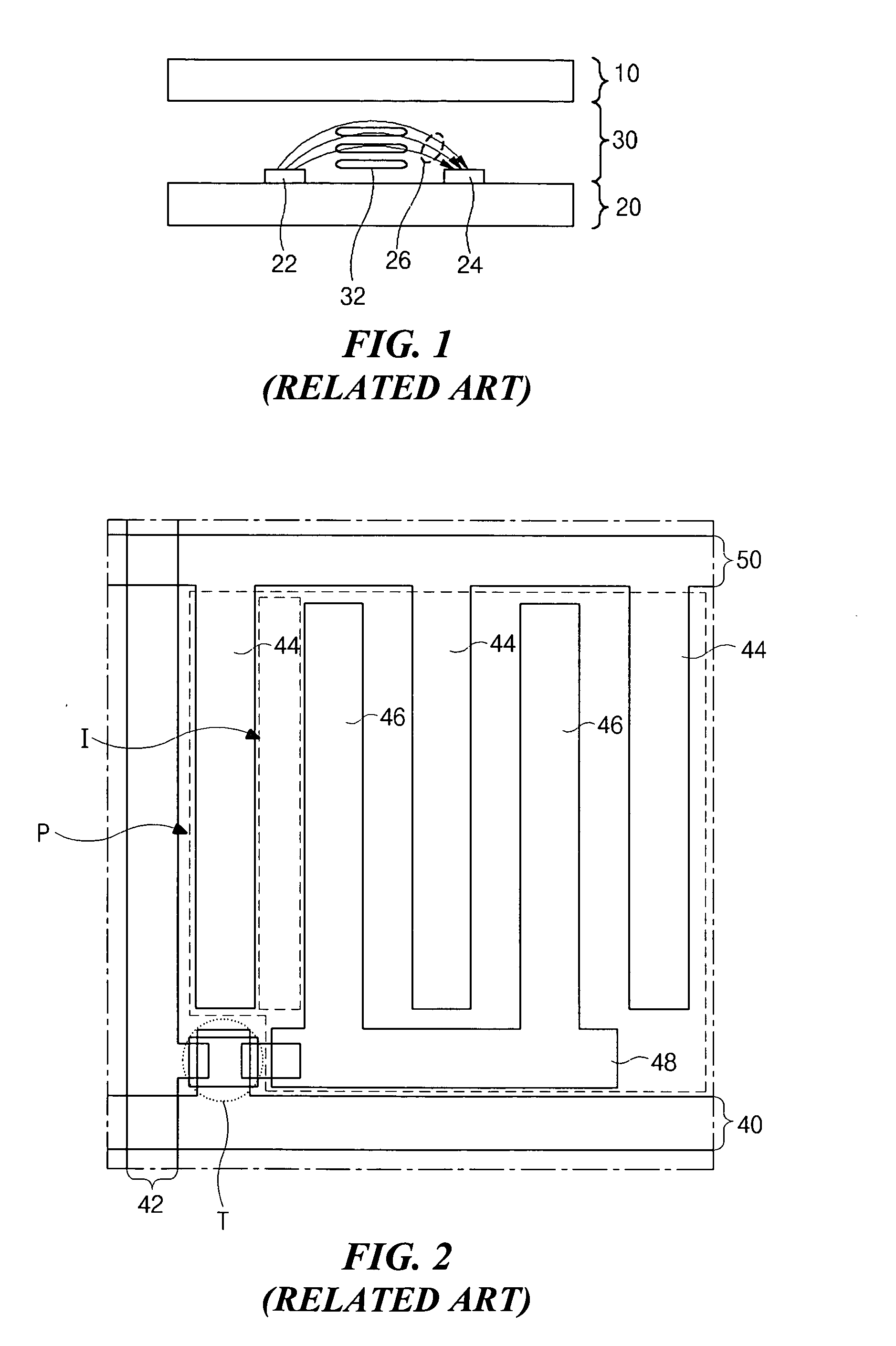
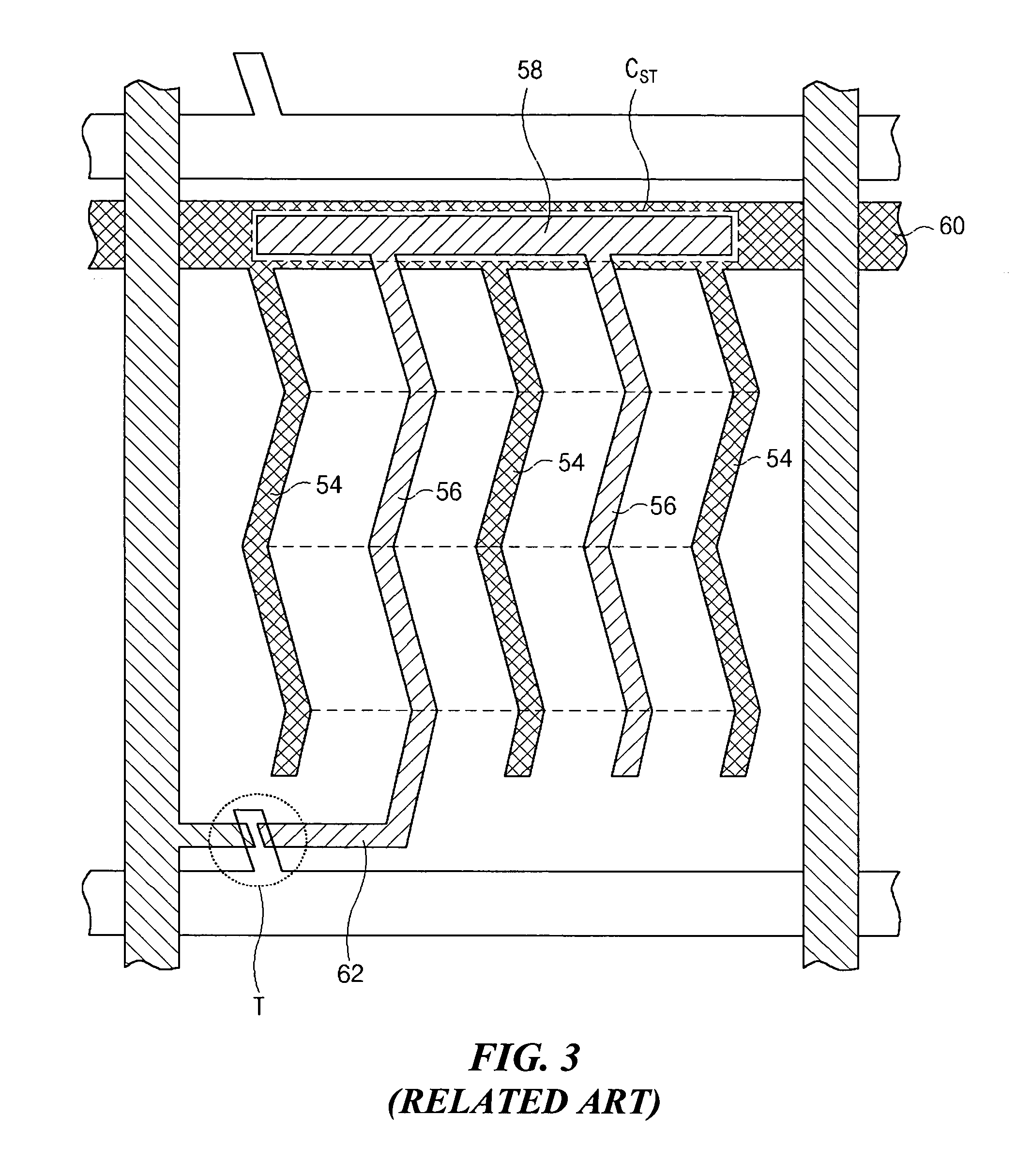
a liquid crystal display and display device technology, applied in non-linear optics, instruments, optics, etc., can solve the problems of multidomains having a color shifting dependent problem, narrow viewing angle, and lcd devices having this perpendicular electric field, so as to prevent cross-talk

Inactive Publication Date: 2005-09-22
LG DISPLAY CO LTD
View PDF10 Cites 9 Cited by
  • Summary
  • Abstract
  • Description
  • Claims
  • Application Information

AI Technical Summary

Benefits of technology

[0020] Another object of the present invention is to provide a liquid crystal display device and a method of fabricating the same to prevent a color shift.

Problems solved by technology

However, the LCD devices having this perpendicular electric field have a drawback in that they have a very narrow viewing angle.
The IPS-LCD device having the above-mentioned multidomains has a problem of color shifting depending on the viewing angles, because the liquid crystal molecules have long and thin shapes.

Method used


Image

  • Liquid crystal display device and method of fabricating the same
  • Liquid crystal display device and method of fabricating the same
  • Liquid crystal display device and method of fabricating the same

Examples


first embodiment

[0045]FIG. 6 is a cross-sectional view of the liquid crystal display device according to the present invention, and shows characteristics of an electric field induced between pixel and common electrodes. As shown in FIG. 6, adjacent data lines 172 are disposed on a first substrate 170, and a pixel region P is defined between the adjacent data lines 172. A common electrode 174 and a pixel electrode 176 are formed in the pixel region P and are spaced apart from each other. The common electrode 174 includes a plurality of common electrode patterns 174a and 174b and the pixel electrode 176 includes a plurality of pixel electrode patterns 176a and 176b. The common electrode patterns 174a and 174b are alternatively arranged with the pixel electrode patterns 176a and 176b. A second substrate 180 is disposed over the first substrate 170 and a liquid crystal layer 190 is interposed between the first and second substrates 170 and 180.

[0046] When a voltage is applied, a lateral electric field ...

second embodiment

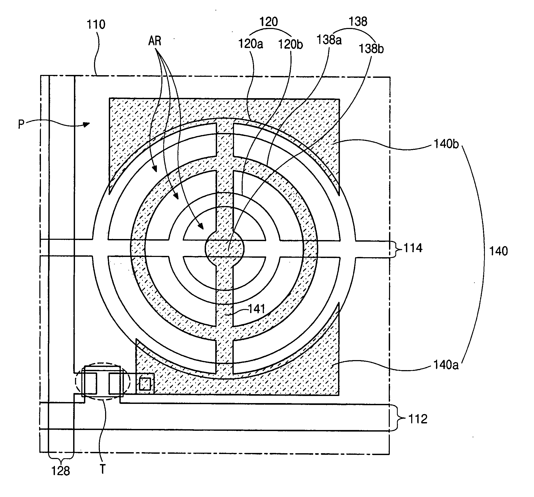
[0048]FIGS. 7A and 7B are plan views illustrating a liquid crystal display device according to the present invention. FIG. 7A shows an array substrate including a thin film transistor and FIG. 7B shows a color filter substrate facing the array substrate. As shown in FIG. 7A, a gate line 212 is formed in a first direction on a first substrate 210 and a data line 228 is formed in a second direction. The gate line 212 and the data line 228 are formed to cross each other and define a pixel region P. A thin film transistor (TFT) T is disposed adjacent to a crossing of the gate line 212 and data line 228.

[0049] A common line 214 is formed in parallel to the gate line 212. A common electrode 220 connected to the common line 214 is formed in the pixel region P. The common electrode 220 includes a first common electrode pattern 220a and a second common electrode pattern 220b extending from the common line 214. The first common electrode pattern 220a is disposed in the outer portion of the pi...

third embodiment

[0060] As shown in FIGS. 9A and 9B, one pixel PX includes four sub-pixels SP(R), SP(G), SP(B) and SP(W) of red, green, blue and white respectively. Each sub-pixel SP(R), SP(G), SP(B) and SP(W) in FIG. 9A has a circular band-shaped pixel electrode and a circular band-shaped common electrode. Each sub-pixel SP(R), SP(G), SP(B) and SP(W) In FIG. 9B just has a circular band-shaped auxiliary common electrode. Because the third embodiment includes a pixel area using sub-pixels with circular shaped electrodes, the aperture ratio is improved.

[0061]FIGS. 10A and 10B are graphs showing brightness properties of IPS LCD devices according to the second and the third embodiments of the present invention, respectively. FIG. 10A shows an IPS LCD device where electrodes are formed on a lower substrate. FIG. 10B shows an IPS LCD device where electrodes are formed on upper and lower substrates, respectively. Here, the IPS LCD devices are normally black mode, and a driving voltage of about 3V is used. ...


PUM

PropertyMeasurementUnit
viewing anglesaaaaaaaaaa
driving voltageaaaaaaaaaa

Abstract

A liquid crystal display device includes: gate lines and data lines on a first substrate, the gate lines and the data lines crossing each other and defining a pixel region; a thin film transistor adjacent to a crossing of the gate and data lines; a common line in parallel to the gate line; a common electrode extending from the common line and having a circular shape; a pixel electrode connected to the thin film transistor and having a circular shape; an auxiliary common line on a second substrate spaced apart from and facing the first substrate; an auxiliary common electrode extending from the auxiliary common line and having a circular shape; and a liquid crystal layer between the first and second substrates.

Description

[0001] This application claims the benefit of Korean Patent Application No. 2003-0092255, filed on Dec. 17, 2003, which is hereby incorporated by reference. BACKGROUND OF THE INVENTION [0002] 1. Field of the Invention [0003] The present invention relates to a liquid crystal display device, and more particularly, to an in-plane switching (IPS) liquid crystal display device and a method of fabricating the same. [0004] 2. Discussion of the Related Art [0005] A liquid crystal display device uses the optical anisotropy and polarization properties of liquid crystal molecules to produce an image. The long and thin shaped liquid crystal molecules can all have the same definite orientational alignment direction. That alignment direction can be controlled by an applied electric field. In other words, as an applied electric field changes, so does the alignment direction of the liquid crystal molecules. Due to optical anisotropy, the refraction of incident light depends on the alignment directi...

Claims


Application Information

Patent Timeline
Patent Type & Authority Applications(United States)
IPC IPC(8): G02F1/1343
CPCG02F1/134363G02F1/1343
Inventor LEE, YUN-BOK
Owner LG DISPLAY CO LTD
Why Eureka
Try Eureka