Device and method for detecting stress migration properties

Inactive Publication Date: 2005-09-29
INFINEON TECH AG
View PDF17 Cites 14 Cited by
  • Summary
  • Abstract
  • Description
  • Claims
  • Application Information

AI Technical Summary

Benefits of technology

[0013] A device and a method are provided for detecting stress migration properties of a semiconductor module finally mounted in a prod

Problems solved by technology

This leads to the contact holes or vias becoming increasingly susceptible to stress migration.
As a result, an electrical resistance of interconnects in the semiconductor module may be increased or even an interconnect interruption may occur.
As a result, after a certain time, usually several months or years, this mass transport in the interconnect layer or the vias produces voids which influence the electrical properties of the semiconductor module and may lead as far as an interruption of an interconnect.
However, in the case of a test device of this type, the results obtained are only inadequate on account of a lack of final mounting in a housing and, in this respect, do not enable a sufficiently accurate detection of the stress migration properties of the semiconductor module in an environment close to the

Method used


Image

  • Device and method for detecting stress migration properties
  • Device and method for detecting stress migration properties
  • Device and method for detecting stress migration properties

Examples


Embodiment Construction

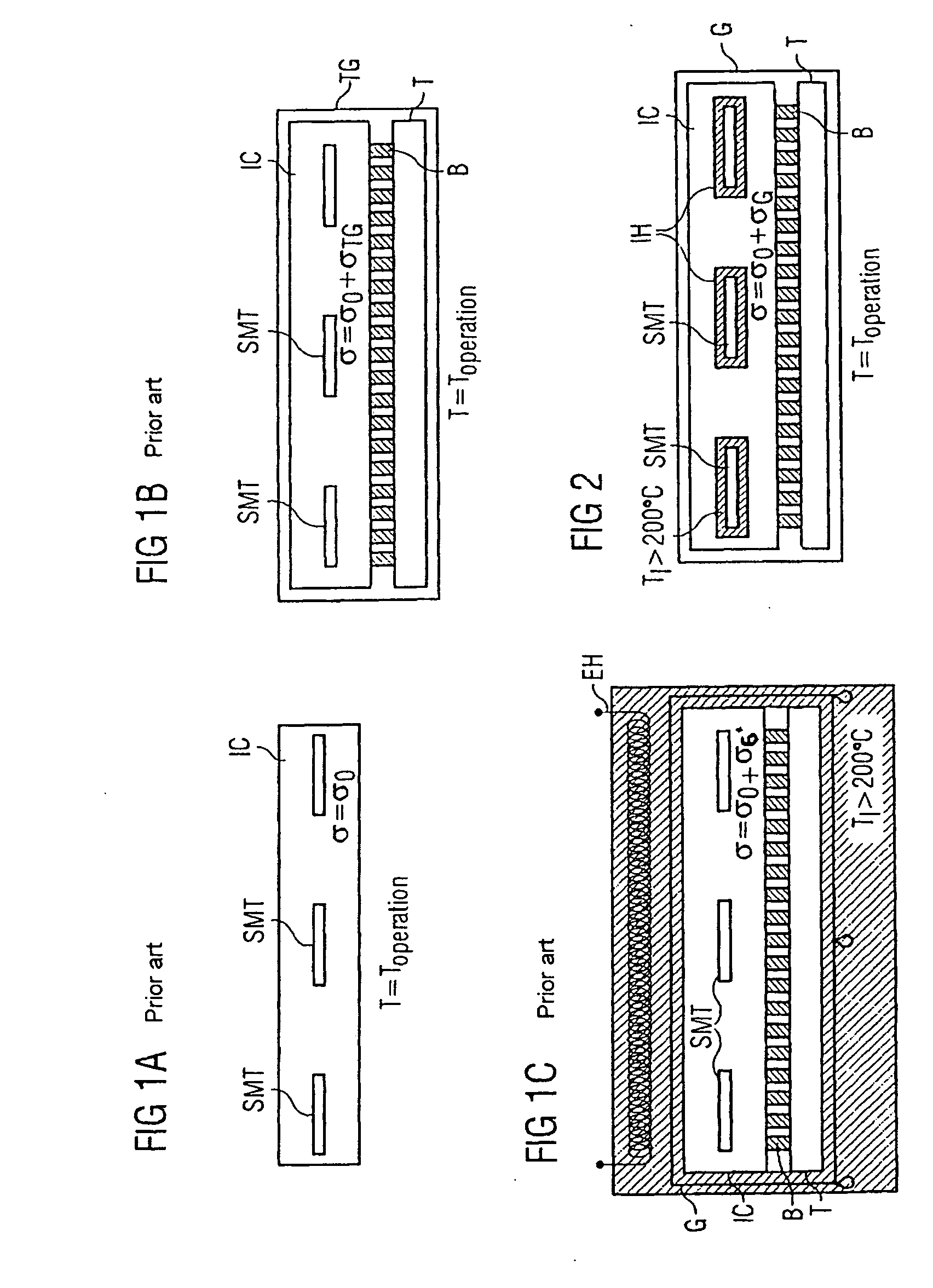
[0030]FIG. 2 shows a simplified sectional view of a device for detecting stress migration properties, identical reference symbols designating elements identical or corresponding to those in FIGS. 1A to 1C and a repeated description being dispensed with below.

[0031] In accordance with FIG. 2, the reliability examinations for characterizing stress migration properties (in particular of metallizations) in semiconductor modules IC (Integrated Circuits) are carried out, according to the invention, in a finally mounted state and after packaging in a product-relevant housing G.

[0032] In the case of so-called flip-chip housings G, in particular, mechanical stresses are induced in the semiconductor module IC right into the region of the yield stress of bulk materials, for which reason they constitute an increased reliability risk. This influence, which cannot be assessed in accordance with the prior art, is detected in accordance with FIG. 2 by virtue of the fact that the stress migration ...


PUM


Abstract

A device and method are provided for detecting stress migration properties of a semiconductor module mounted in a housing. A stress migration test (SMT) structure is formed in the semiconductor module. An integrated heating (IH) device is formed within or in direct proximity to the SMT structure. The SMT structure includes a first interconnect region in a first interconnect layer, a second interconnect region in a second interconnect layer, and a connecting region electrically connecting the interconnect regions through a first insulating layer. The IH device includes a heating interconnect region through which a heating current flows. The heating interconnect region is within or outside the first or second interconnect region or connecting region. When the heating current is applied, a measurement voltage is applied to the SMT structure, and a current through the SMT structure is measured to detect stress migration properties of the semiconductor module.

Description

PRIORITY [0001] 100011 This application is a continuation of International Application PCT / DE03 / 03844, filed on Nov. 20, 2003, which claims the benefit of priority to German Patent Application 102 54 756.4, filed on Nov. 23, 2002, incorporated herein by referenceTECHNICAL FIELD [0002] The present invention relates to a device and a method for detecting stress migration properties and in particular to a device and a method for detecting stress migration properties of a semiconductor module mounted in a product-relevant housing. BACKGROUND [0003] Integrated circuits are usually fabricated with a multiplicity of patterned metallization or interconnect planes which are electrically isolated from one another by dielectric intermediate insulating layers. In order to realize electrical connections between the patterned metallization or interconnect layers or between the interconnect layers and a substrate, contact holes or vias are formed in the insulating layer at selected locations. [000...

Claims


Application Information

Patent Timeline
IPC IPC(8): H01L21/66H01L23/544H01L23/58
CPCH01L22/34H01L2924/0002H01L2924/00
Inventor FISCHER, ARMINVON GLASOW, ALEXANDERVON HAGEN, JOCHEN
Owner INFINEON TECH AG
Why Eureka
Try Eureka