

Fabrication of nanoelectronic circuits
a technology of nanoelectronic circuits and fabrication lines, applied in the direction of photomechanical equipment, instruments, photosensitive material processing, etc., can solve the problem of not being able to register patterns to one another with such accuracy, and achieve ultra-high accuracy alignment and removal of ion beam damage
Inactive Publication Date: 2005-09-29
NEWSOUTH INNOVATIONS PTY LTD
View PDF5 Cites 0 Cited by
- Summary
- Abstract
- Description
- Claims
- Application Information
AI Technical Summary
Benefits of technology
[0031] Annealing the sample to activate the dopants and remove ion-beam damage.
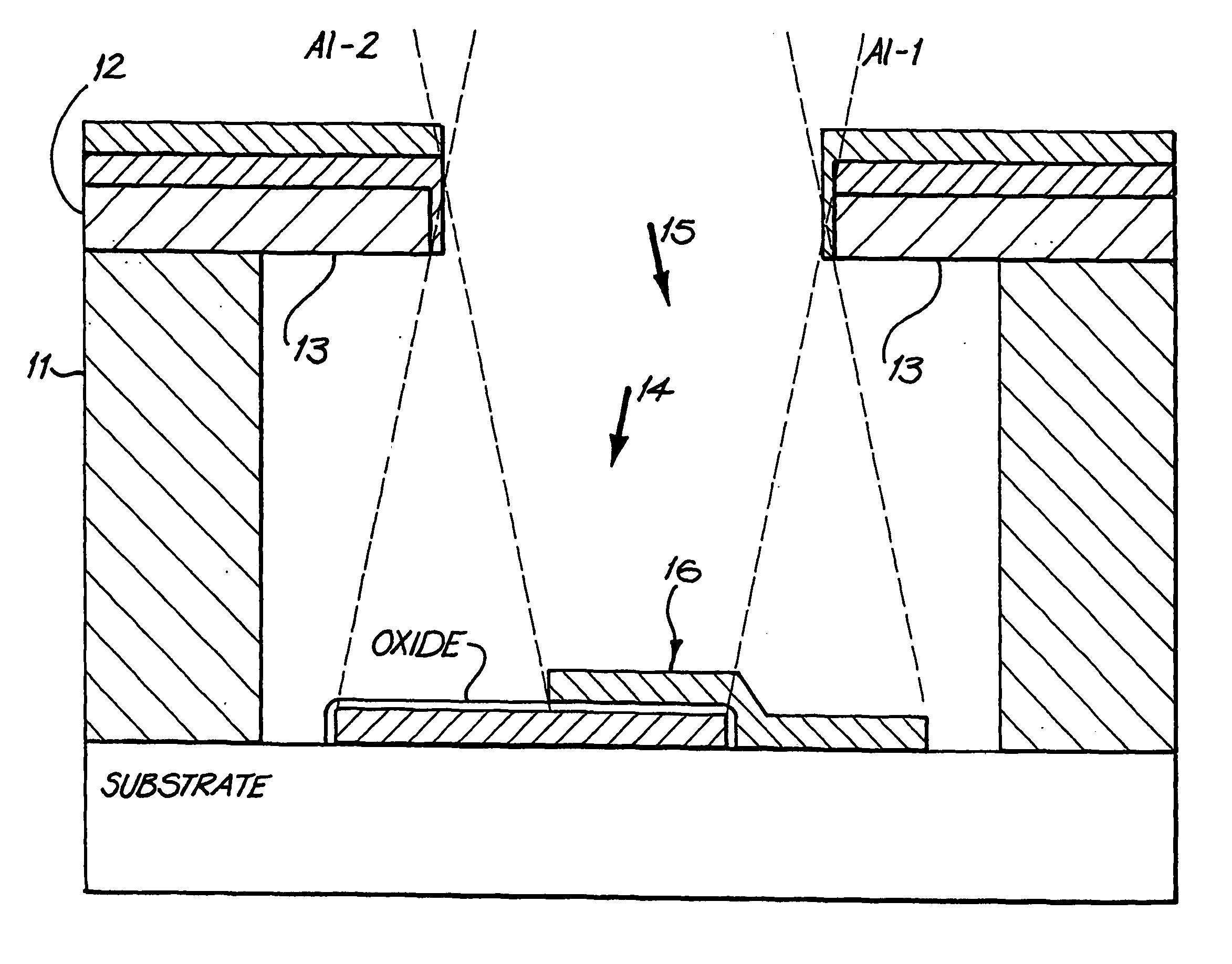
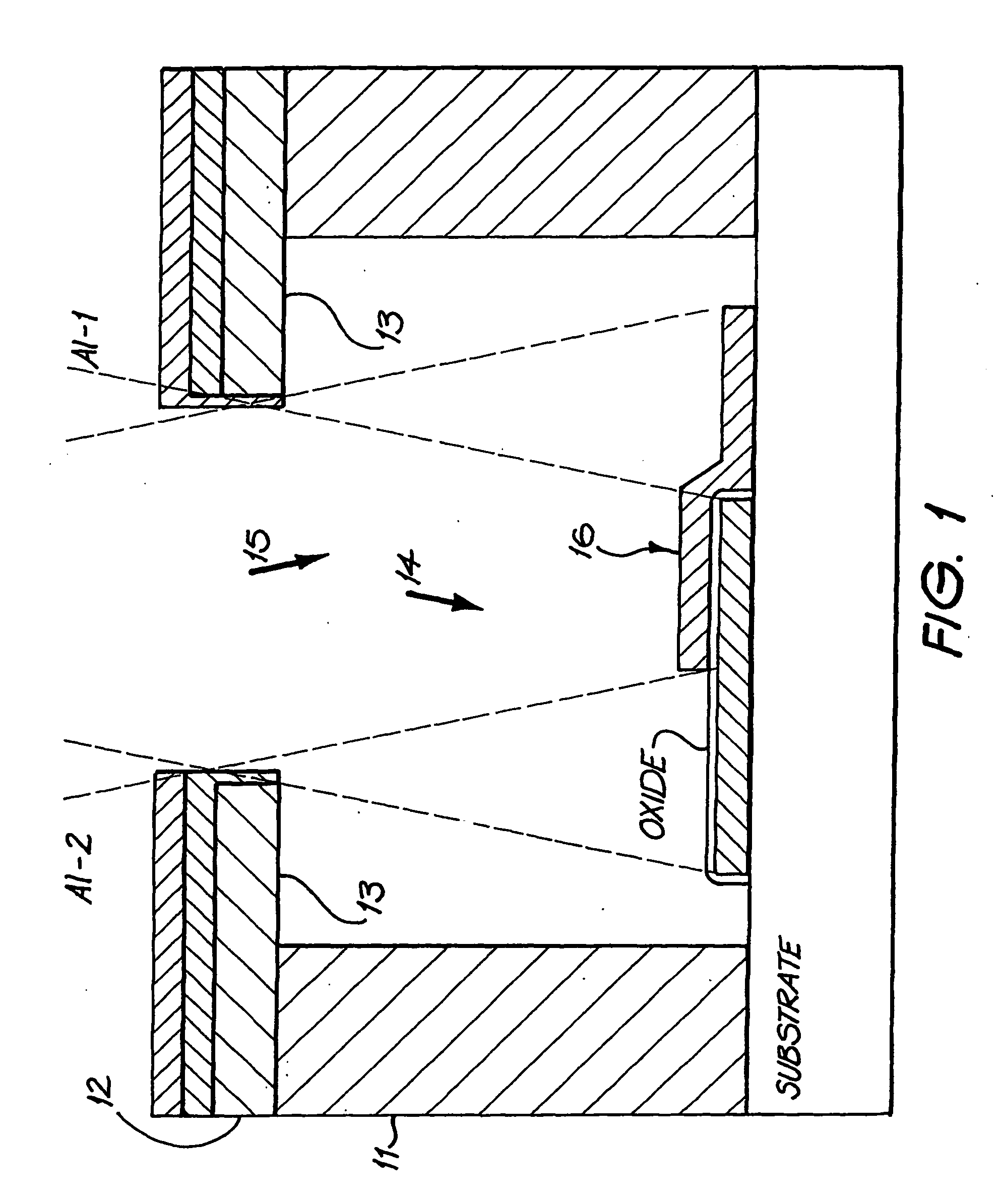
[0032] In the case of electron beam lithography (EBL) alignment is limited by the ability to focus on registration features at the low beam currents needed for high-resolution pattern exposure. Consequently, it is difficult to achieve alignment better than 50 nm, which would not be sufficient for SSQC devices. The key advantage of the double exposure process described here is that ultra-high accuracy alignment is not required. The crossed exposure patterns create a mask for subsequent ion implantation which is perfectly aligned to the control gates in one direction. Alignment in the direction perpendicular to this is far less critical. In addition
Problems solved by technology
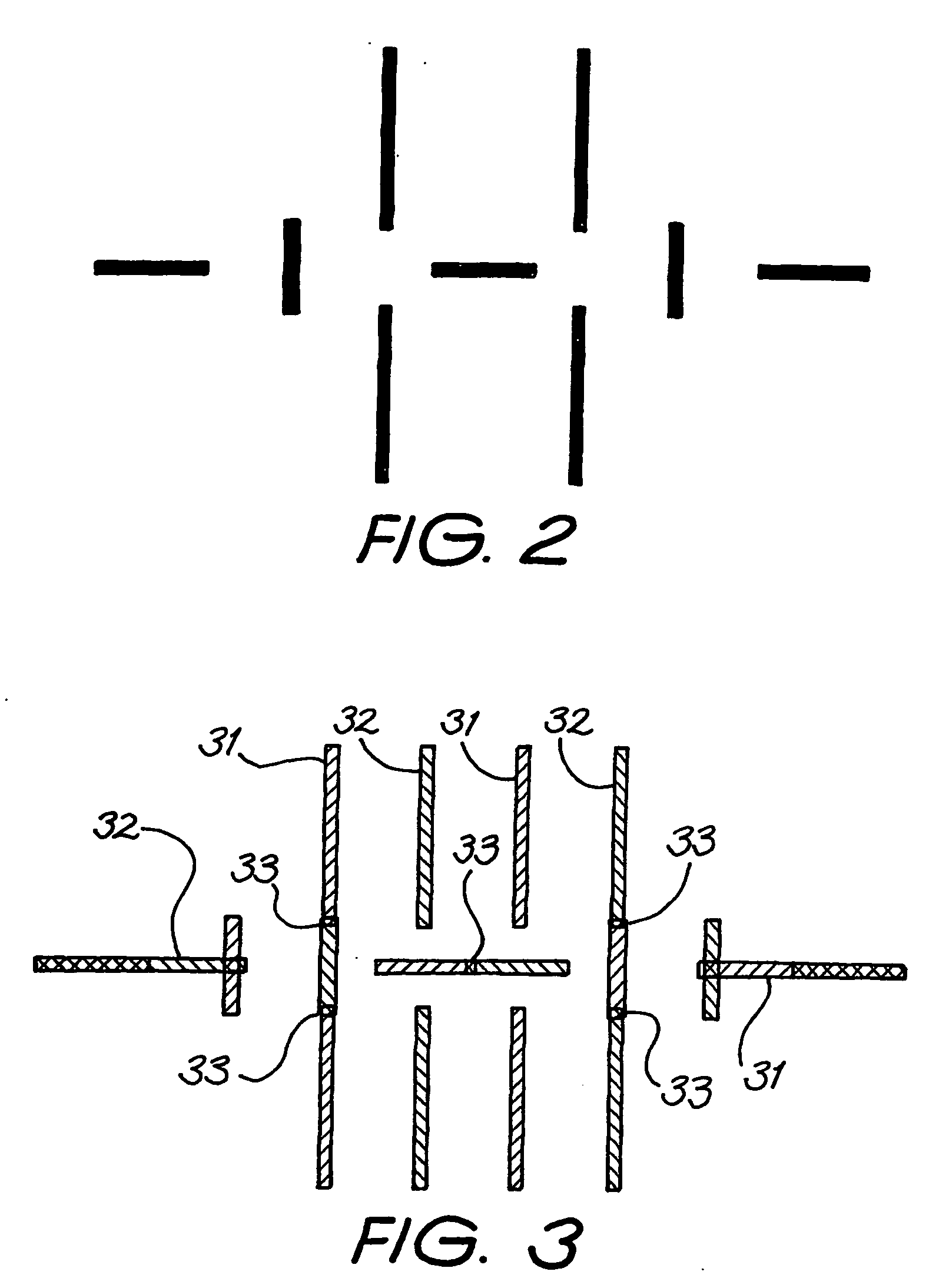
Both circuit patterns can be written with the same resolution and accuracy as each othe
Method used
View moreImage
Smart ImageViewing Examples

Examples
 PUM
 Abstract
A silicon substrate is coated with one or more layers of resist. First and second circuit patterns are exposed in sequence, where the second pattern crosses the first pattern. The patterned resist layers are developed to open holes which extend down to the substrate only where the patterns cross over each other. These holes provide a mask suitable for implanting single phosphorous ions in the substrate, for a solid state quantum computer. Further development of the resist layers provides a mask for the deposition of nanoelectronic circuits, such as single electron transistors, aligned to the phosphorous ions.
Description
TECHNICAL FIELD [0001] This invention concerns the fabrication of nanoelectronic circuits, and in particular methods of fabrication of nanoelectronic circuits suitable for solid state quantum computer control and read-out. In a further aspect it concerns circuits made using the method. BACKGROUND ART [0002] One proposed architecture for fabricating a solid state quantum computer (SSQC), involves an array of phosphorous-31 (31 P) atoms embedded in a silicon matrix to provide the quantum bits (qubits). In this design1,2 the qubit information is encoded on the nuclear spin of the phosphorous atoms, which have a very long spin relaxation time at low temperatures. Interactions between qubits is mediated via the donor electrons associated with the phosphorous atoms, which can be conveniently controlled using gate electrodes. Alternatively the qubit information can simply be encoded on the electron spin3, although in this case the quantum computation is more susceptible to decoherence erro...
Claims
Login to View More Application Information
Patent Timeline
 IPC IPC(8): G03F7/20G03F7/26G06N99/00H01L21/027H01L21/266H01L21/335H01L21/336H01L29/66H01L29/78H01L49/00
CPCB82Y10/00G06N99/002H01L49/006H01L29/66439H01L21/266G06N10/00H10N99/05
InventorBRENNER, ROLFBUEHLER, TILO MARCUSCLARK, ROBERT GRAHAMDZURAK, ANDREW STEVENHAMILTON, ALEXANDER RUDOLFLUMPKIN, NANCY ELLENPAYTRICIA, RITA
OwnerNEWSOUTH INNOVATIONS PTY LTD