Integrated circuit having one or more conductive devices formed over a SAW and/or MEMS device

a technology of integrated circuits and saws, which is applied in the direction of semiconductor devices, semiconductor/solid-state device details, electrical apparatus, etc., can solve the problems of undesirably large die sizes, saw or mems devices are generally not integrated on the same chip, and other conductors and devices cannot be easily formed above saw or mems devices

Inactive Publication Date: 2005-09-29
MONTEREY RES LLC +1
View PDF55 Cites 27 Cited by
  • Summary
  • Abstract
  • Description
  • Claims
  • Application Information

AI Technical Summary

Problems solved by technology

One challenge associated with both SAW and MEMS devices is that free areas are needed for the mechanical properties of the devices.
Because of this restriction, other conductors and devices cannot be easily formed above SAW or MEMS devices.
Consequently, SAW or MEMS devices are generally not integrated on the same chip with other conductive structures.
In cases in which additional conductors or circuits are fabricated on the same chip as SAW or MEMS devices, the additional devices must be laterally disposed across the chip, leading to undesirably large die sizes.
Another predicament with SAW and MEMS devices is that the active regions of the devices can be very sensitive to the presence of surface contaminants.
Surface contaminants may, for example, alter the wave velocities of a SAW device or modify the voltage level at which a moving part with a MEMS device is brought into contact or released from a contact pad.
As a consequence, device performance may be degraded for the SAW device or MEMS device.
Even a monolayer of contaminant on the surface of a SAW or MEMS device can noticeably alter device performance.

Method used


Image

  • Integrated circuit having one or more conductive devices formed over a SAW and/or MEMS device
  • Integrated circuit having one or more conductive devices formed over a SAW and/or MEMS device
  • Integrated circuit having one or more conductive devices formed over a SAW and/or MEMS device

Examples


Embodiment Construction

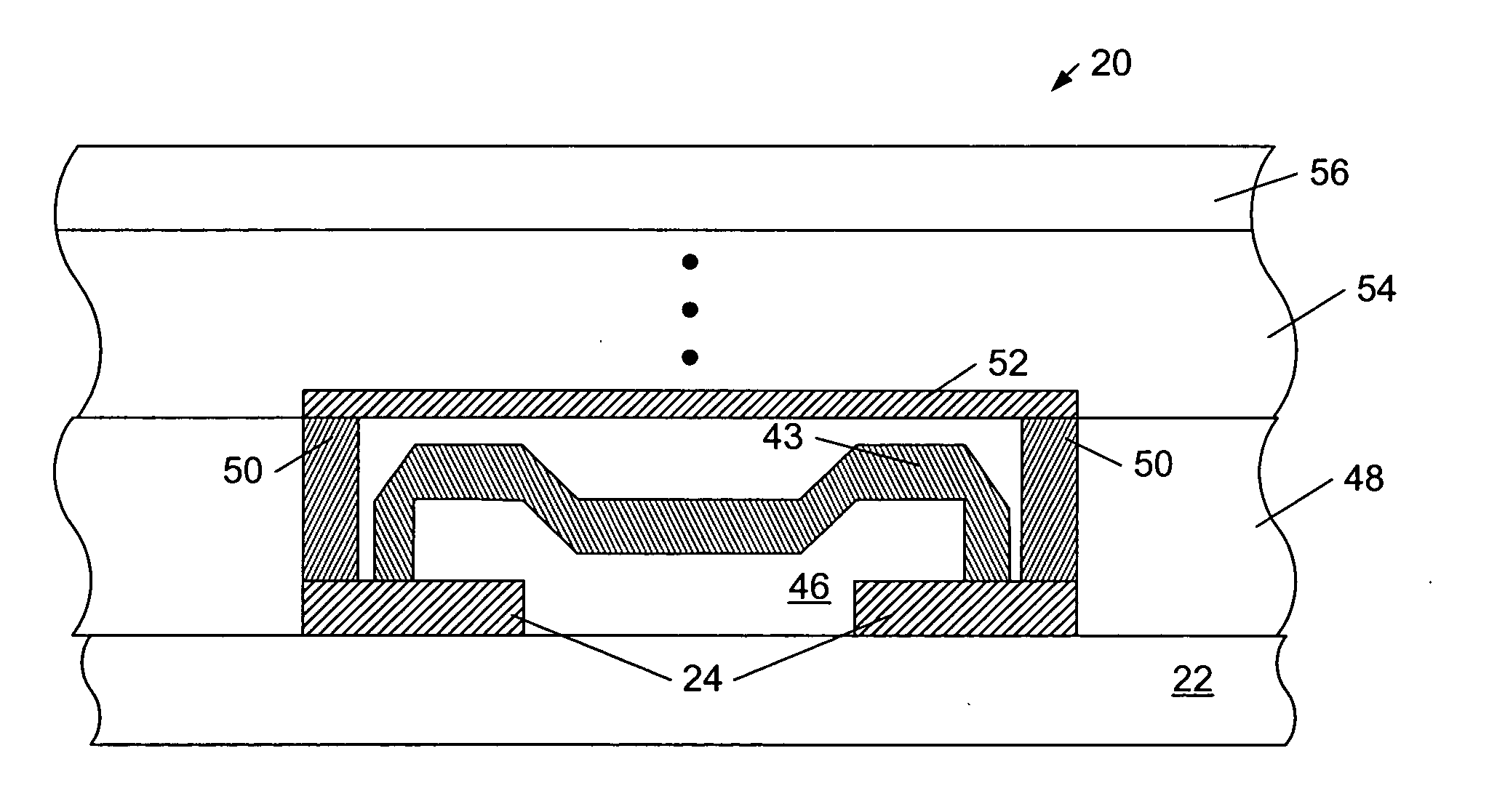
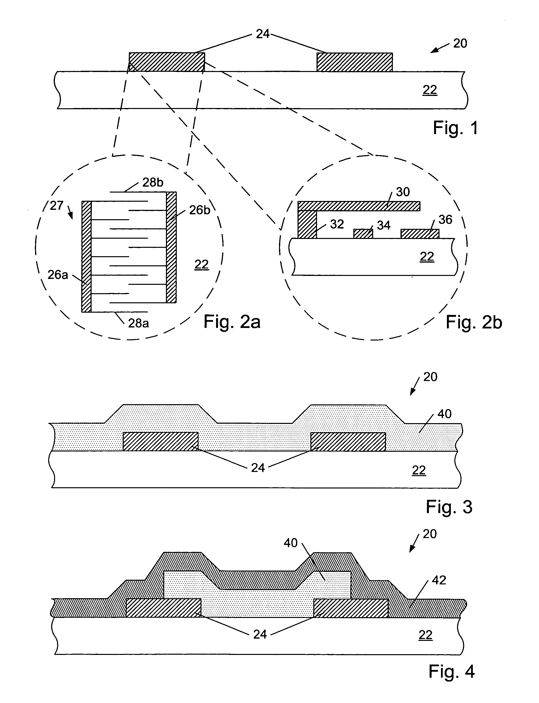
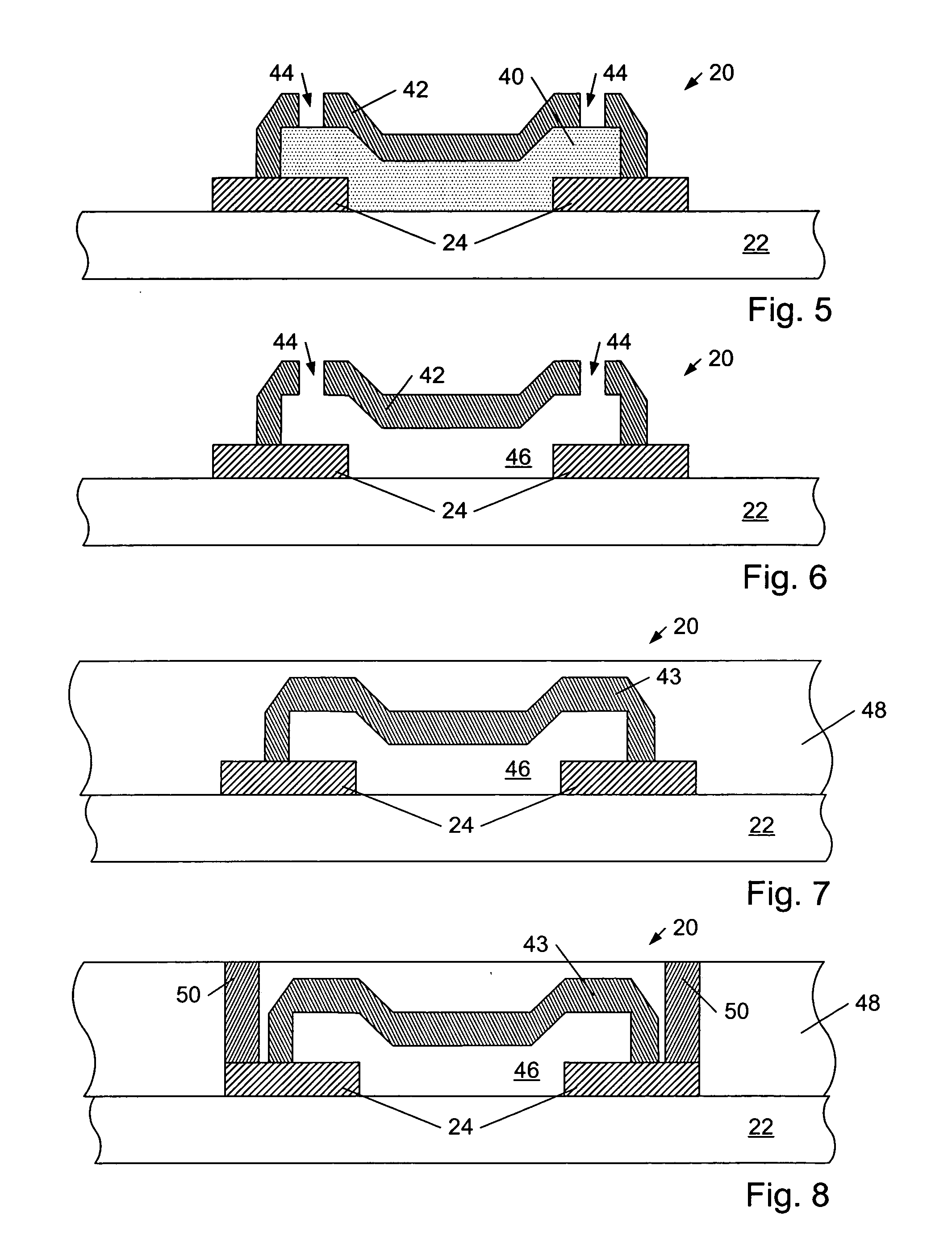
[0027] Turning to the drawings, an exemplary method for fabricating an integrated circuit including a surface acoustic wave (SAW) device and / or a micro electromechanical system (MEMS) device having one or more conductive devices formed thereover is provided. In particular, FIGS. 1-10 depict a process in which one or more device elements of a SAW device and / or a MEMS device are formed within a sealed cavity and one or more conductive features are formed thereover. As shown in FIG. 1, topography 20 includes device elements 24 arranged upon base substrate 22. As described in more detail below, device elements 24 are general reference blocks representing one of more conductive features of a SAW device or a MEMS device. In reference thereto, it is noted that the components of topography 20 are not drawn to scale in FIG. 1 nor in FIGS. 2-11. For instance, the aggregate thickness of components among each of device elements 24 may be on the order of thousands of angstroms to a few microns, ...


PUM


Abstract

An integrated circuit is provided which includes one or more device elements formed above a base substrate, a structure forming a sealed cavity above at least a portion of the one or more device elements, and one or more conductive devices formed above the sealed cavity. A method for fabrication of such an integrated circuit is also provided. An exemplary embodiment of the integrated circuit includes a surface acoustic wave device having a plurality of tracks each with a first interdigitated transducer configured to convert a receiving electric field energy into mechanical wave energy and a second interdigitated transducer configured to convert the mechanical wave energy into an output electric field energy. The SAW device also includes a conductor arranged above and spanning across at least two tracks of the plurality of tracks and coupled to the first interdigitated transducers of at least the two tracks.

Description

PRIORITY APPLICATION [0001] The present application claims priority to provisional application No. 60 / 556,812 entitled “Multiple Level Conductors on SAW or MEM Devices,” filed Mar. 26, 2004.BACKGROUND OF THE INVENTION [0002] 1. Field of the Invention [0003] The present invention relates generally to microelectronic device fabrication and, more particularly, the fabrication of a SAW device and / or a MEMS device having one or more conductive devices formed thereover. [0004] 2. Description of the Related Art [0005] The following descriptions and examples are given as background information only. [0006] Microelectronic devices have been developed for a diversity of applications using a variety of technologies. Some exemplary microelectronic devices include surface acoustic wave (SAW) devices and micro electromechanical system (MEMS) devices. SAW devices exploit the propagation properties of waves along the surface or the near surface of a substrate. Changes in velocity and / or amplitude o...

Claims


Application Information

Patent Timeline
Patent Type & Authority Applications(United States)
IPC IPC(8): H01L21/425H01L21/50H03H3/007H03H3/08H03H9/00H03H9/05H03H9/10H03H9/64
CPCH03H3/0073H03H3/08H03H9/0085H03H9/14588H03H9/1057H03H9/1064H03H9/1092H03H9/0547
Inventor FIELD, DEAN L.STONE, CHARLES N.BRUNER, MICHAEL W.
Owner MONTEREY RES LLC
Why Eureka
Try Eureka