Memory module with parallel testing

a memory module and parallel testing technology, applied in the field of memory modules, can solve the problems of increasing the complexity of data analysis within the test system, increasing the number of pins, etc., and achieve the effect of more efficient testing

Inactive Publication Date: 2005-09-29
SAMSUNG ELECTRONICS CO LTD
View PDF10 Cites 5 Cited by
  • Summary
  • Abstract
  • Description
  • Claims
  • Application Information

AI Technical Summary

Benefits of technology

[0018] In this manner, the memory module simultaneously tests a total of N test data bits from X memory blocks but outputs N / X test data bits. Thus, the test system processes less data bits (N / X test data bits) even though the memory module simultaneously tests a total of N test data bits for more efficient testing.

Problems solved by technology

Thus, the total number of data values stored and output by output buffer units 40 to the test system increases disadvantageously resulting in increased number of pins and increased complexity of data analysis within the test system.
However, the conventional parallel testing apparatus 100 does not output any data bits from the memory device 10.

Method used


Image

  • Memory module with parallel testing
  • Memory module with parallel testing
  • Memory module with parallel testing

Examples


Embodiment Construction

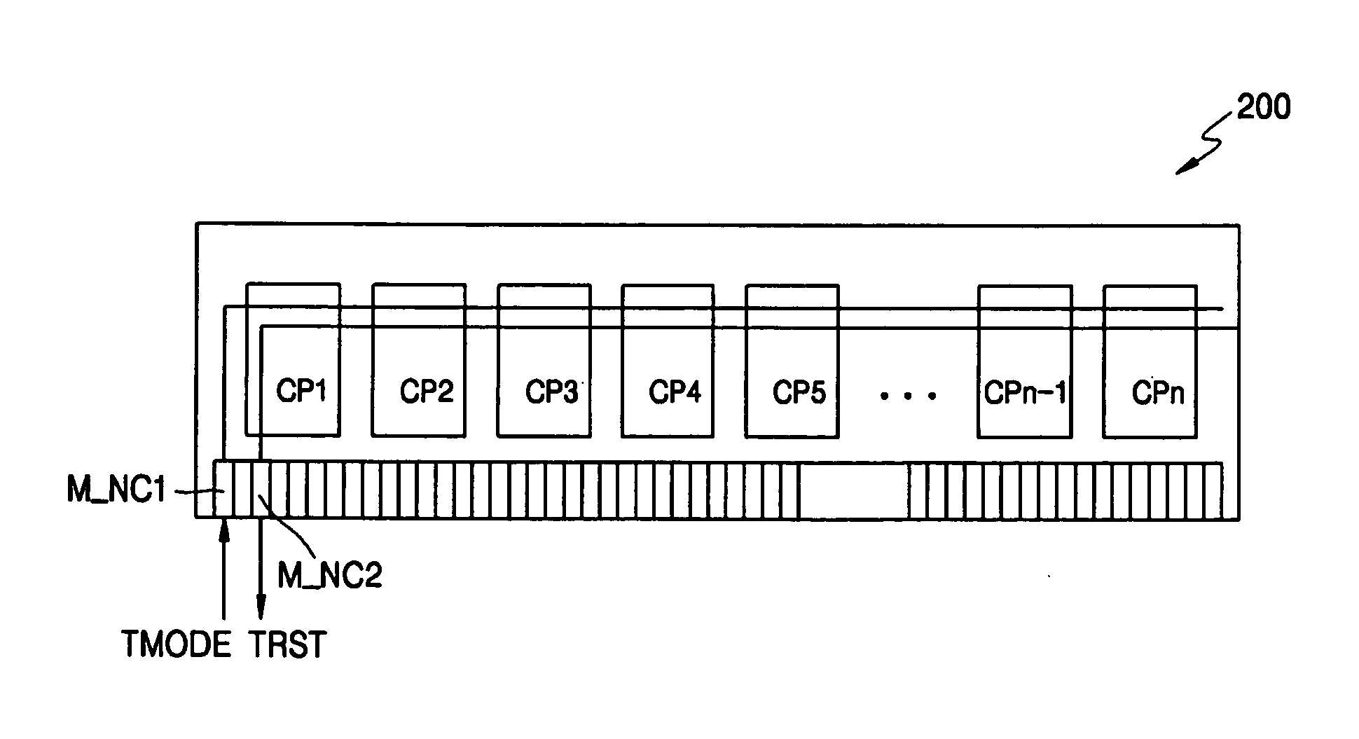
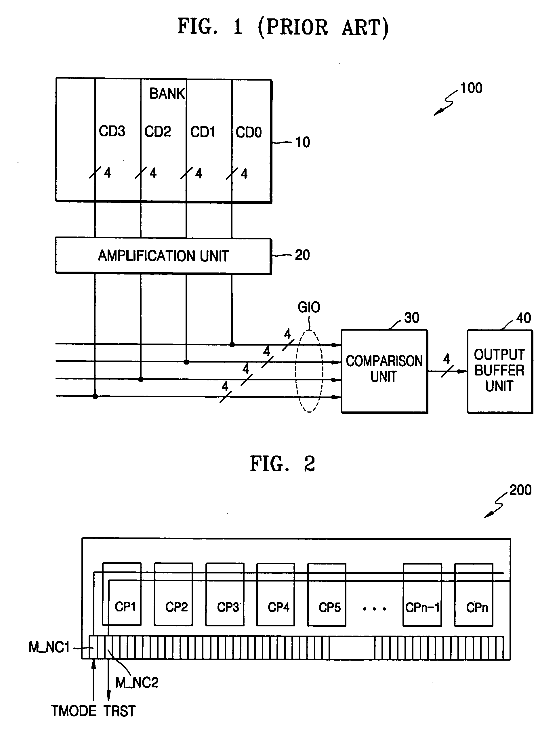
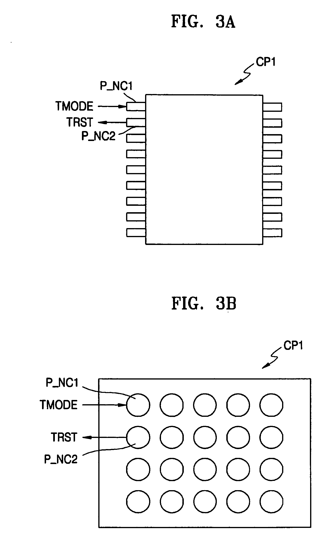
[0032] Referring to FIG. 2, a memory module 200 includes a plurality of memory chips CP1, CP2, . . . , and CPn, a first module no-connection (NC) pin M_NC1, and a second module NC pin M_NC2. FIG. 3A shows one of the memory chips of FIG. 2 with a pin structure, and FIG. 3B shows one of the memory chips of FIG. 2 with a ball structure.

[0033] Referring to FIGS. 2, 3A, and 3B, the first module NC pin M_NC1 receives a test mode signal TMODE and couples the test mode signal TMODE to a respective first NC pin P_NC1 of each of the memory chips CP1 through CPn. The second module NC pin M_NC2 receives a respective test result signal TRST from the second NC pin P_NC2 of each of the memory chips CP1 through CPn. The respective TRST signal indicates whether each of the memory chips CP1 through CPn is defective.

[0034] When the TMODE signal is activated (to a logical high state “1”), the memory module 200 performs parallel testing to be descried herein. When the TMODE signal is deactivated (to a...


PUM


Abstract

Each memory chip of a memory module tests a total of N data bits from X memory blocks for efficient testing and outputs N/X test data bits from one of the memory blocks. A memory module includes a plurality of memory chips and a plurality of comparison units. Each comparison unit is disposed within a respective memory chip for testing a plurality of test data bits from a plurality of memory blocks. In addition, each comparison unit outputs test data bits from one of the memory blocks within the respective memory chip.

Description

BACKGROUND OF THE INVENTION [0001] This application claims priority to Korean Patent Application Nos. 2004-19628 filed on Mar. 23, 2004, and 2004-70025 filed on Sep. 2, 2004, in the Korean Intellectual Property Office, the disclosures of which are incorporated herein in their entirety by reference. [0002] 1. Field of the Invention [0003] The present invention relates generally to memory modules, and more particularly, to parallel testing within a memory module for increased efficiency. [0004] 2. Description of the Related Art [0005]FIG. 1 shows a conventional parallel testing apparatus 100 for a semiconductor memory device 10. Referring to FIG. 1, the conventional parallel testing apparatus 100 includes an amplification unit 20, global input / output lines (GIO), a comparison unit 30, and an output buffer unit 40. The amplification unit 20 amplifies data received from memory cells of the memory bank 10. [0006] The amplified data is coupled to the comparison unit 30 via the global inpu...

Claims


Application Information

Patent Timeline
Patent Type & Authority Applications(United States)
IPC IPC(8): G01R31/28G06F11/00G06F12/16G11C29/00G11C29/28G11C29/34G11C29/40
CPCG11C29/28G11C2029/2602G11C29/40
Inventor KIM, YOUN-CHEULCHOI, HEE-JOOHA, KAE-WONLEE, JOON-HEE
Owner SAMSUNG ELECTRONICS CO LTD
Why Eureka
Try Eureka