Liquid crystal display device and method of manufacturing liquid crystal display device

a liquid crystal display and liquid crystal technology, applied in static indicating devices, instruments, non-linear optics, etc., can solve the problems of easy breakage of the layer structure, unsuitable liquid crystal for the display of moving images,

Inactive Publication Date: 2005-10-06
FUJITSU LTD
View PDF10 Cites 42 Cited by
  • Summary
  • Abstract
  • Description
  • Claims
  • Application Information

AI Technical Summary

Benefits of technology

[0035] The above and further objects and features of the invention will more fully be apparent from the following detailed description with accompanying drawings.
[0036]FIG. 1 is a schematic plan view showing a conventional liquid crystal panel;
[0037]FIG. 2 is a schematic plan view showing one example of a liquid crystal panel according to Embodiment 1 of the present invention;
[0038]FIG. 3 is a structural cross-sectional view along the II-II line of FIG. 2;
[0039]FIG. 4 is a schematic plan view showing another example of a liquid crystal panel according to Embodiment 1 of the present invention;
[0040]FIGS. 5A through 5F are views for explaining a method of manufacturing a liquid crystal panel by sticking an array substrate and a counter substrate together;

Problems solved by technology

Consequently, when displaying moving images (for example, 60 images per second) on a liquid crystal display device using a TN liquid crystal, the liquid crystal molecules can not move sufficiently and the images are blurred, and therefore the TN liquid crystal is not suitable for the display of moving images, such as multimedia applications.
If the FLC is used as a liquid crystal substance, there is a drawback that the layer structure is easily broken by stress applied to the liquid crystal substance, such as an external force that changes the gap.

Method used


Image

  • Liquid crystal display device and method of manufacturing liquid crystal display device
  • Liquid crystal display device and method of manufacturing liquid crystal display device
  • Liquid crystal display device and method of manufacturing liquid crystal display device

Examples


embodiment 1

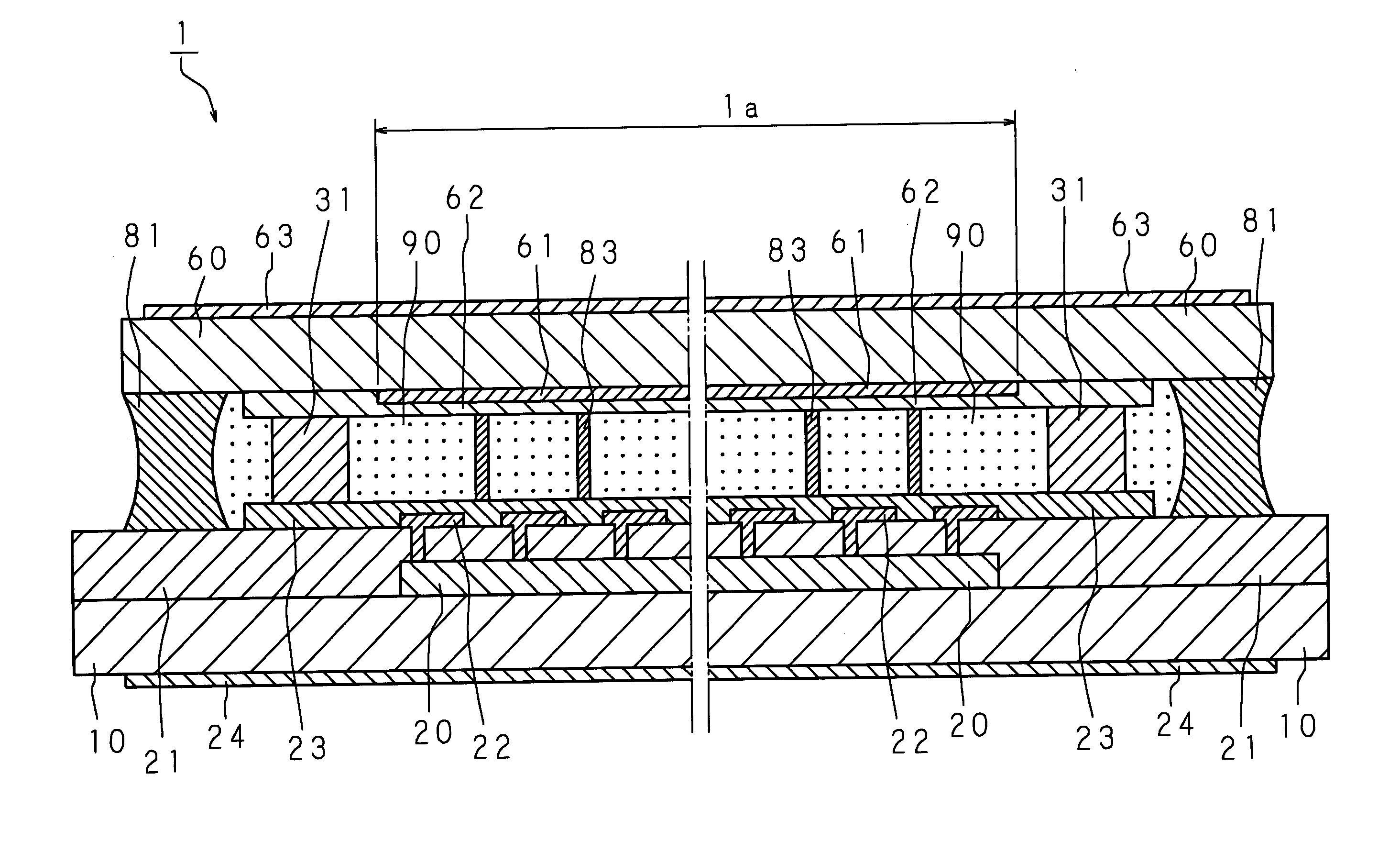
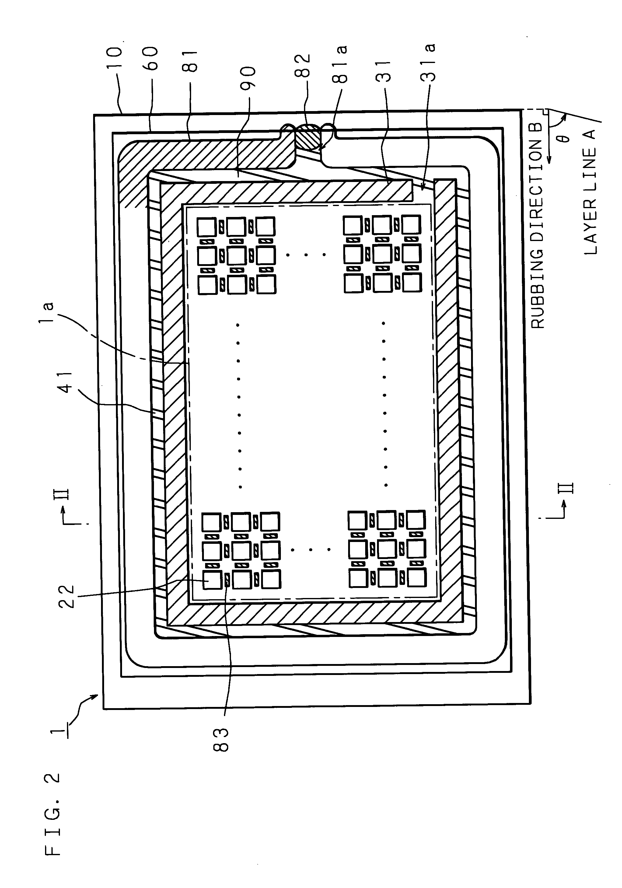
[0050]FIG. 2 is a schematic plan view showing one example of a liquid crystal panel according to Embodiment 1 of the present invention, and FIG. 3 is a structural cross-sectional view along the II-II line of FIG. 2. In order to facilitate understanding, a part of the components is not illustrated in FIG. 2. A liquid crystal panel 1 according to Embodiment 1 of the present invention comprises an array substrate 10 and a counter substrate 60 functioning as insulating substrates made of glass or quartz with good transmittance in the visible light region. The peripheral portions of the array substrate 10 and the counter substrate 60 are sealed with a seal member 81 and a closing member 82, and a gap formed by sealing is filled with a liquid crystal substance 90 such as a mono-stable (one-side-stable) ferroelectric liquid crystal material composition.

[0051] A TFT layer 20 constituting a TFT matrix is formed in a display region 1a of the array substrate 10, and a 2.5 μm flattening film 2...

embodiment 2

[0065] In Embodiment 1, the position of the aperture portion 31a provided in the partition wall 31 is determined according to the layer line A of the liquid crystal substance so as to prevent the defects 41 that occur in the seal member 81 from entering the display region 1a, but the position of the aperture portion 31a may be located at any position on the liquid crystal inlet 81a side, and Embodiment 2 illustrates such an example. FIG. 6 is a schematic plan view showing one example of a liquid crystal panel according to Embodiment 2 of the present invention, and a part of the components is not illustrated in FIG. 6 to facilitate understanding.

[0066] A liquid crystal panel 2 according to Embodiment 2 of the present invention has a partition wall 32 inside the seal member 81, that is, on the display region 2a side, and the partition wall 32 has an aperture portion 32a produced by opening the center of a side on the liquid crystal inlet 81a side so as to guide the liquid crystal sub...

embodiment 3

[0071] In Embodiments 1 and 2, the partition walls 31 and 32 having the aperture portions 31a and 32a with small size are provided, but, it may also be possible to provide the partition wall with a large aperture portion, for example, in the shape of letter “C”, and Embodiment 3 illustrates such an example. FIG. 7 is a schematic plan view showing one example of a liquid crystal panel according to Embodiment 3 of the present invention, and a part of the components is not illustrated in FIG. 7 to facilitate understanding.

[0072] A liquid crystal panel 3 according to Embodiment 3 of the present invention has a C-shaped partition wall 33 inside the seal member 81, that is, on the display region 3a side, and the partition wall 33 is placed so that its aperture portion 33a is open in the liquid crystal inlet 81a side to guide the liquid crystal substance 90 to the display region 3a in the liquid crystal injection step. Since other structures are the same as those of Embodiment 1, the corr...


PUM

PropertyMeasurementUnit
thicknessaaaaaaaaaa
width×12aaaaaaaaaa
widthaaaaaaaaaa

Abstract

In a liquid crystal display device, one or a plurality of partition walls adhering to the two substrates are provided in a region between the adhesive member for sealing the peripheral portions of the two substrates and a display region located inside the adhesive member so as to reduce stress applied to the liquid crystal substance. Even when stress is applied to the liquid crystal substance in the peripheral portion of the substrate, the stress is reduced by the partition wall and is not transmitted to the display region on the opposite side of the partition wall. Therefore, even when a crack occurs in the peripheral portion of the substrate due to the stress, the propagation of the crack is stopped by the partition wall, and the crack does not enter the display region.

Description

CROSS-REFERENCE TO RELATED APPLICATIONS [0001] This non-provisional application claims priority under 35 U.S.C. §119(a) on Patent Application No. 2004-105453 filed in Japan on Mar. 31, 2004, the entire contents of which are hereby incorporated by reference.BACKGROUND OF THE INVENTION [0002] The present invention relates to a liquid crystal display device and a method of manufacturing a liquid crystal display device, and more specifically relates to a liquid crystal display device capable of reducing stress applied to a liquid crystal substance and preventing display defects caused by the stress, and a method of manufacturing the liquid crystal display device. [0003] Along with the recent development of office automation systems, office automation (OA) apparatuses such as word processors, personal computers and PDA (Personal Digital Assistants) have been widely used. With the spread of such OA apparatuses, portable OA apparatuses that can be used in offices as well as outdoors are us...

Claims


Application Information

Patent Timeline
Patent Type & Authority Applications(United States)
IPC IPC(8): G02F1/133G02F1/1339G02F1/1341G02F1/141
CPCG02F1/1339G02F1/141G02F1/13394
Inventor TADAKI, SHINJIKIYOTA, YOSHINORIYOSHIHARA, TOSHIAKISHIROTO, HIRONORIMAKINO, TETSUYAKASAHARA, SHIGEOBETSUI, KEIICHI
Owner FUJITSU LTD
Why Eureka
Try Eureka