Dark field inspection system

a technology of inspection system and dark field, applied in the field of optical inspection, can solve problems such as reducing process yield, and achieve the effect of high resolution and higher data collection ra

Active Publication Date: 2005-10-06
APPLIED MATERIALS INC +1
View PDF12 Cites 93 Cited by
  • Summary
  • Abstract
  • Description
  • Claims
  • Application Information

AI Technical Summary

Benefits of technology

[0010] Embodiments of the present invention provide improved methods and apparatus for dark-field inspection of a surface of a sample, such as a semiconductor wafer, which enable such surfaces to be inspected with high resolution, at much higher rates of data collection than in systems known in the art.
[0024] In some embodiments, the radiation source is adapted to emit pulsed radiation, and the image sensors are adapted to form the respective images in synchronization with the pulsed radiation. The radiation source may include a pulsed laser, which is adapted to emit the radiation in pulses shorter than 1 μs in duration, and a speckle-reduction module, which is coupled to de-correlate the radiation so as to reduce a contrast of speckles formed on the area to less than 10%. Preferably, the speckle-reduction module is adapted to reduce the contrast of the speckles to no more than about 1%. In a disclosed embodiment, the speckle-reduction module includes one or more fiberoptic bundles. In another embodiment, the speckle-reduction module includes an opto-electronic transducer, which is coupled to scan an incidence angle of a beam of the radiation over a target plane during each of the pulses so as to de-correlate the radiation. Typically, the laser is adapted to lase in multiple transverse modes simultaneously, and the speckle-reduction module is adapted to mix the transverse modes in order to reduce the contrast of the speckles.
[0027] Typically, each of the image processing channels is adapted to correct coordinates of pixels in the images formed by the respective one of the sensor arrays, so as to compensate for optical distortion in the images due to the respective angular range of the scattered radiation. Each of the image processing channels may be adapted to detect locations of deviations in the images formed by the respective one of the sensor arrays relative to a predefined reference, and to correct the coordinates of the pixels at the locations of the deviations for output to the multi-perspective processor, without correcting the coordinates of at least some other pixels in the images.

Problems solved by technology

Defects can cause device failures, thus substantially reducing the process yield.

Method used


Image

  • Dark field inspection system
  • Dark field inspection system
  • Dark field inspection system

Examples


Embodiment Construction

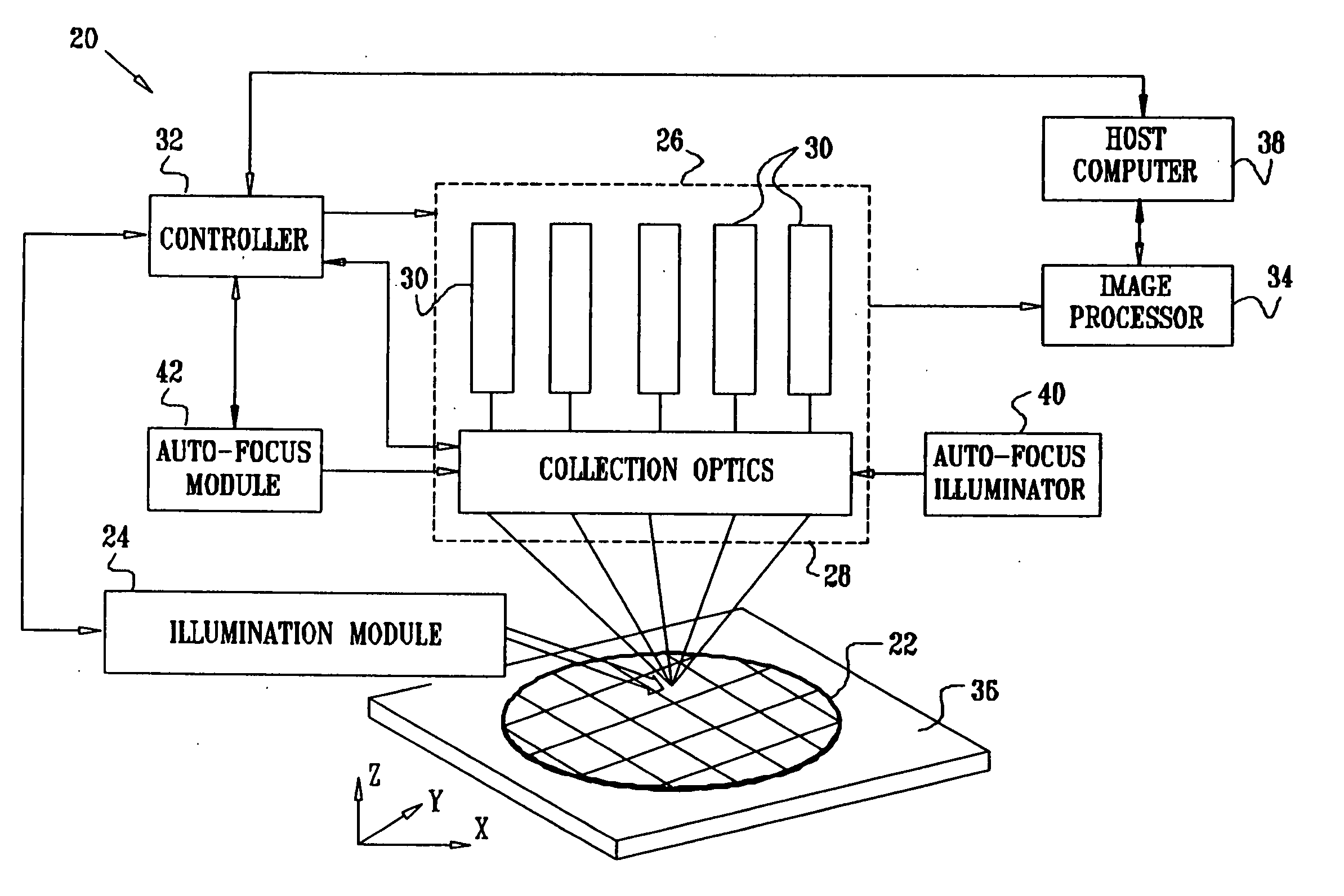
[0046]FIG. 1 is a block diagram that schematically illustrates a system 20 for optical inspection of a semiconductor wafer 22, in accordance with an embodiment of the present invention. Typically, wafer 22 is patterned, using methods of semiconductor device production known in the art, and system 20 applies dark-field optical techniques to detect defects on the surface of the wafer. Alternatively, however, the principles embodied in system 20 may be applied to unpatterned wafers and to inspection of other types of samples and surfaces, as well, such as masks and reticles. Furthermore, although system 20 is dedicated to dark-field inspection, aspects of the present invention may also be applied in bright-field inspection, as well as in other areas of illumination, inspection and imaging.

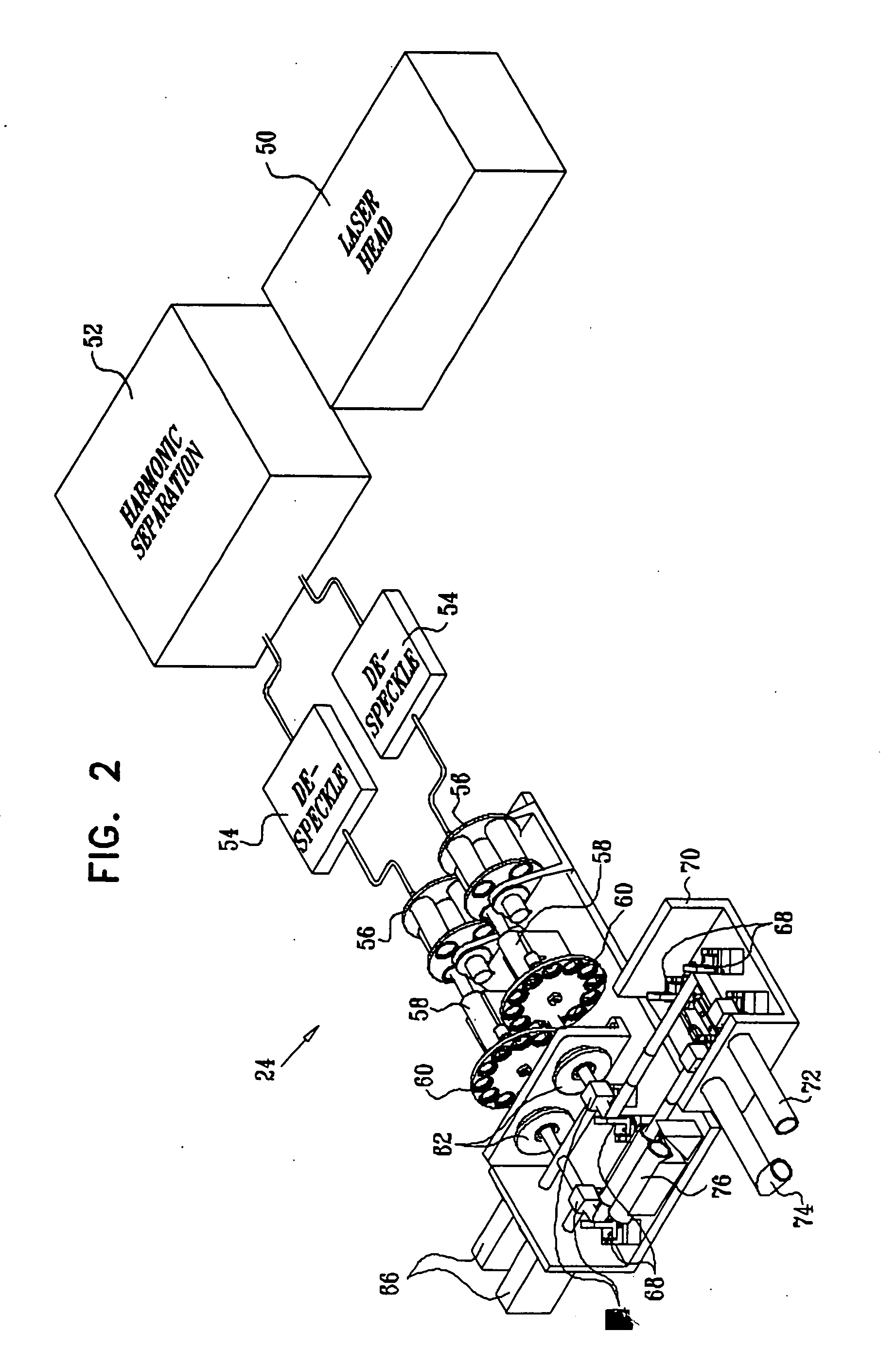
[0047] System 20 comprises an illumination module 24, which illuminates the surface of sample 22 using pulsed laser radiation. Typically, module 24 is able to emit the laser radiation selectably at t...


PUM

PropertyMeasurementUnit
sizeaaaaaaaaaa
sizeaaaaaaaaaa
angleaaaaaaaaaa

Abstract

Apparatus for inspection of a sample includes a radiation source, which is adapted to direct optical radiation onto an area of a surface of the sample, and a plurality of image sensors. Each of the image sensors is configured to receive the radiation scattered from the area into a different, respective angular range, so as to form respective images of the area. An image processor is adapted to process at least one of the respective images so as to detect a defect on the surface.

Description

CROSS-REFERENCE TO RELATED APPLICATIONS [0001] This application is related to two other U.S. patent applications, filed on even date, entitled “Illumination System for Optical Inspection” and “Inspection System with Oblique Viewing Angle.” Both of these related applications are incorporated herein by reference. FIELD OF THE INVENTION [0002] The present invention relates generally to optical inspection, and specifically to methods and apparatus for inspection of solid-state surfaces, such as semiconductor wafers, and detection of features and defects thereon. BACKGROUND OF THE INVENTION [0003] Optical inspection is commonly used in semiconductor device manufacturing to detect defects on the surface of a wafer, such as contaminant particles, scratches and unremoved portions of material layers. Defects can cause device failures, thus substantially reducing the process yield. Therefore, careful inspection is required to verify the cleanliness and quality both of unpatterned wafers and o...

Claims


Application Information

Patent Timeline
Patent Type & Authority Applications(United States)
IPC IPC(8): G01N21/47G01N21/88G01N21/95G01N21/956G02B27/48
CPCG01N21/47G01N2201/0697G01N21/8806G01N21/94G01N21/9501G01N21/95607G01N21/95623G01N2021/1772G01N2021/4711G01N2021/4735G01N2021/479G01N2021/4792G01N2021/8822G01N2021/8845G01N21/4788H01S3/005
Inventor KORNGUT, DORONADMONI, EREZKADAR, OFERHAIKOVIZ, LEVFELDMAN, HAIMGUETTA, AVISHAY
Owner APPLIED MATERIALS INC
Why Eureka
Try Eureka