

Method of improving the uniformity of a patterned resist on a photomask
Patent Information
- Authority / Receiving Office
- US · United States
- Current Assignee / Owner
- APPLIED MATERIALS INC
- Publication Date
- 2005-10-06
- Estimated Expiration
- Not applicable · inactive patent
Smart Images
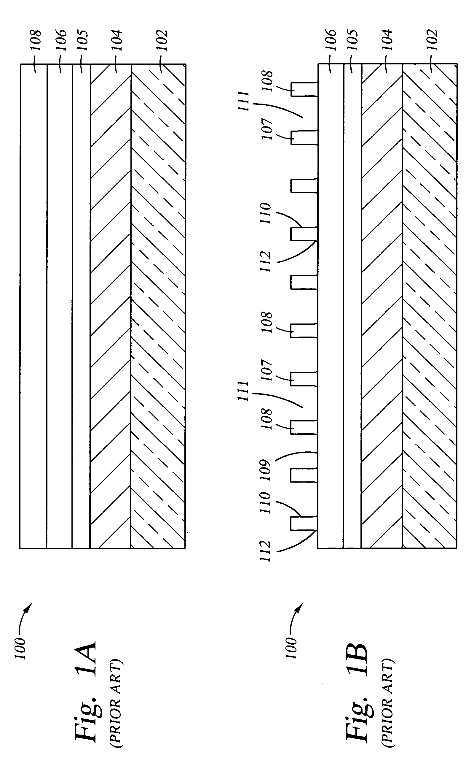
Figure 1 
Figure 2 
Figure 3
Abstract
Description
[0001] 1. Field of the Invention
[0002] In general, the present invention relates to a method of producing a photomask (reticle) for use in the semiconductor industry. In particular, the invention pertains to a method for improving the critical dimension (CD) uniformity of a pattern in a photoresist which is used to transfer the pattern to a reticle.
[0003] 2. Brief Description of the Background Art
[0004] Photoresists are used in microlithographic processes to produce patterned features required for device functioning in miniaturized electronic components, such as in the fabrication of semiconductor device structures. The miniaturized electronic device structure patterns are typically created using blanket radiation through a photomask to produce a pattern in a layer of photoresist material present on a semiconductor structure. There are instances, for specialized devices, where a pattern is directly written into a photoresist present on the semiconductor structure; however, due to...