Light-emitting diode array having an adhesive layer

a technology of light-emitting diodes and adhesive layers, which is applied in the field of light-emitting diodes, can solve the problem that the led array disclosed in the patent cannot be applied to a quaternary al—in—ga—p light-emitting diodes

Active Publication Date: 2005-10-13
EPISTAR CORP
View PDF6 Cites 133 Cited by
  • Summary
  • Abstract
  • Description
  • Claims
  • Application Information

AI Technical Summary

Problems solved by technology

However, the LED array disclosed by the patent cannot be applied to a quaternary Al—In—Ga—P light-emitting diode, which comprises a conductive substrate rather than an insulating substrate, P-contacts formed on one side of the conductive substra

Method used


Image

  • Light-emitting diode array having an adhesive layer
  • Light-emitting diode array having an adhesive layer
  • Light-emitting diode array having an adhesive layer

Examples


Embodiment Construction

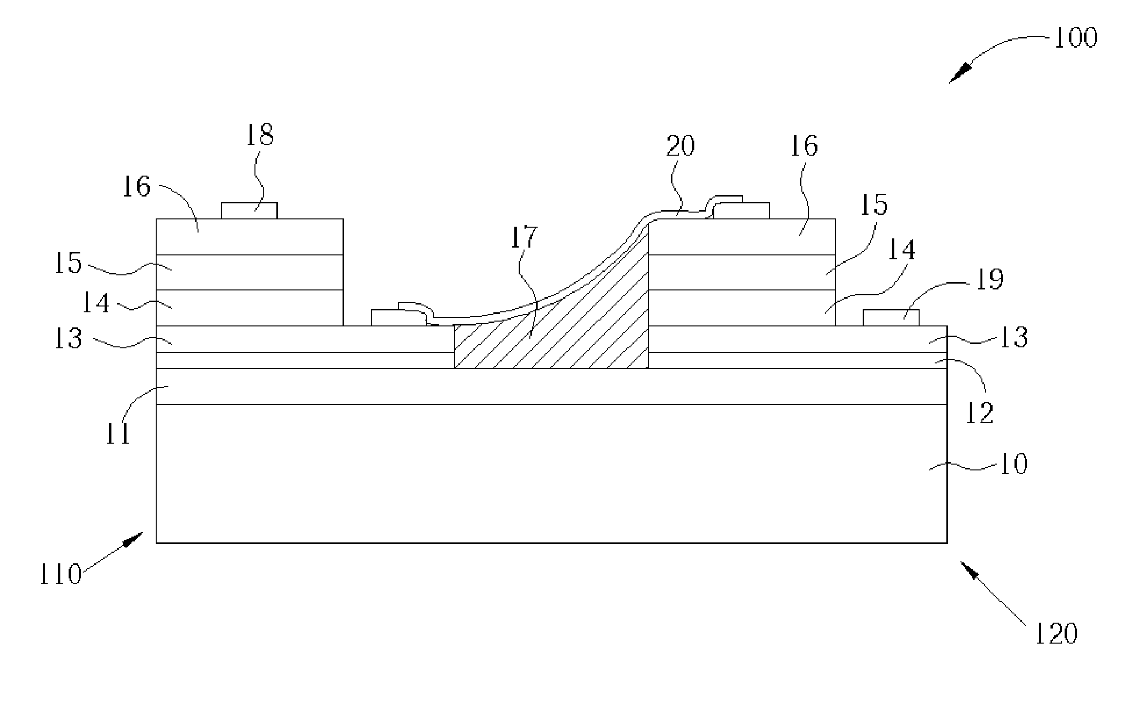
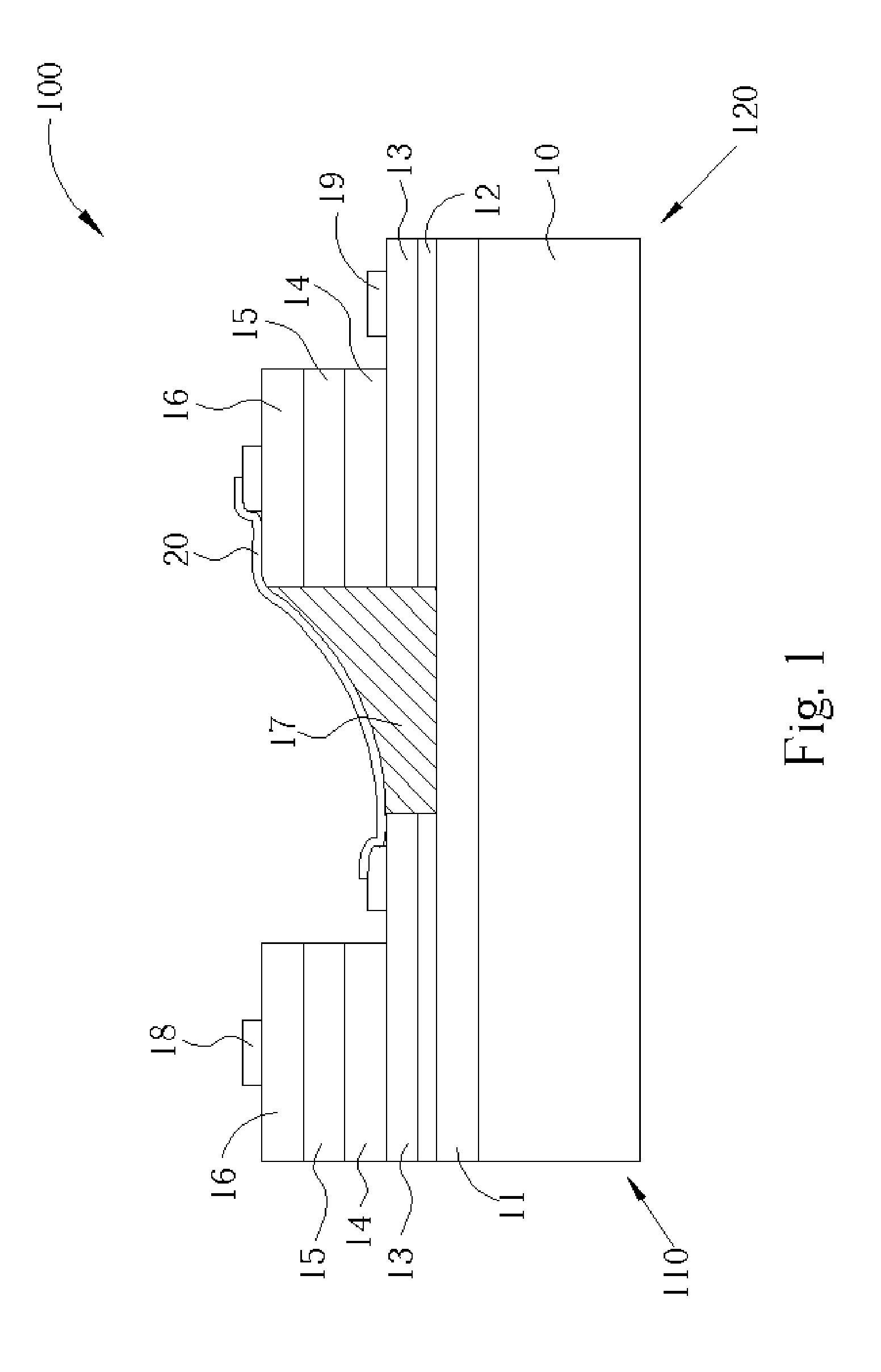
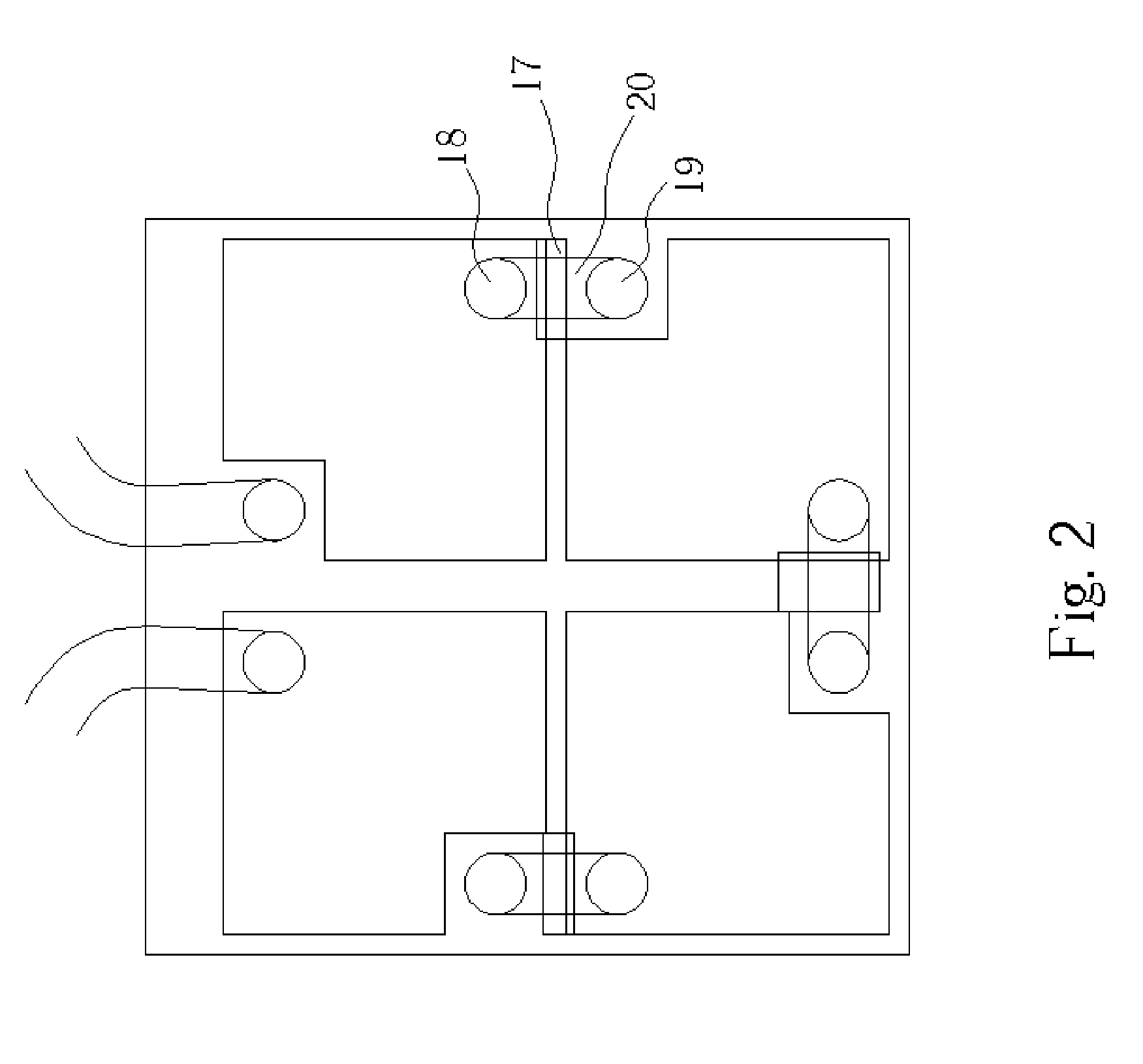
[0016] Please refer to FIG. 1, which is a cross sectional schematic diagram of a light-emitting diode array 100 of the preferred embodiment according to the present invention. The LED array 100 comprises a substrate 10, a reflective layer 11 formed on the substrate 10, an insulating transparent adhesive layer 12 formed on the reflective layer 11, a transparent conductive layer 13 formed on the insulating transparent adhesive layer 12, a first conductive semiconductor stack layer 14 formed on the transparent conductive layer 13, a light-emitting layer 15 formed on the first conductive semiconductor stack layer 14, a second conductive semiconductor stack layer 16 formed on the light-emitting layer 15.

[0017] A trench is formed by etching away a portion of the second conductive semiconductor stack layer 16, the light-emitting layer 15, the first conductive semiconductor stack layer 14, the transparent conductive layer 13, and the insulating transparent adhesive layer 12 sequentially, a...


PUM


Abstract

A light-emitting diode array includes a substrate, an adhesive layer formed on the substrate, and a plurality of electrically connected epitaxial light-emitting stack layer disposed on the adhesive layer. Each of the epitaxial light-emitting stack layer has a P-contact and an N-contact coplanar to the P-contact. The light-emitting diode array has improved heat ventilation characteristics.

Description

BACKGROUND OF INVENTION [0001] 1. Field of the Invention [0002] The present invention relates to a light-emitting diode, and more particularly, to a light-emitting diode array having an adhesive layer. [0003] 2. Description of the Prior Art [0004] Light-emitting diodes (LEDs) are employed in a wide variety of applications including optical display devices, traffic lights, data storage equipment, communications devices, illumination apparatuses, and medical treatment equipment. One of the most important goals of engineers who design LEDs is to increase the brightness of the light emitted. [0005] U.S. Pat. No. 6,547,249 discloses monolithic serial / parallel LED arrays formed on highly resistive substrates. According to the patent, a Group III-V nitride light-emitting stack layer is formed on an insulating substrate. A portion of the stack layer is etched away to form a trench, and in result to form the LED array, which includes a plurality of light-emitting diodes divided by the trench...

Claims


Application Information

Patent Timeline
IPC IPC(8): H01L23/12H01L33/08H01L25/075H01L31/036H01L29/15F21K7/00H01L27/15H01L33/10H01L33/32H01L33/00H01L29/04H01L33/28
CPCH01L25/0753H01L24/24H01L2924/0002H01L2924/12041H01L2924/00
Inventor LIU, WEN-HUANG
Owner EPISTAR CORP
Why Eureka
Try Eureka