Liquid crystal display apparatus and method of driving the same

a technology of liquid crystal display and display apparatus, which is applied in the direction of instruments, computing, electric digital data processing, etc., can solve the problems of affecting the display effect, so as to reduce the brightness difference and flicker of the in-plane, the effect of high brightness and high contras

Inactive Publication Date: 2005-10-13
NEC LCD TECH CORP
View PDF32 Cites 60 Cited by
  • Summary
  • Abstract
  • Description
  • Claims
  • Application Information

AI Technical Summary

Benefits of technology

[0032] In view of the foregoing, an object of the present invention is to provide a method for driving a fast response liquid crystal display apparatus, which method decreases in-plane brightness difference and flicker caused by employment of reset pulses, and which realizes high contrast and high brightness.

Problems solved by technology

This results in the problem that response of liquid crystal generally occurs after completion of signal write operation.
Such a decrease in the holding voltage; i.e., a decrease in the effective applied voltage, results in insufficient writing, so that the on-screen contrast decreases.
Since the liquid crystal requires a few frames to change its transmittance as described above, high speed display of images is impossible.
This is observed as flicker, which has the effect of deteriorating the quality of display.
Even if any of the reset pulse schemes described above is employed, the conventional reset pulse method has the following problems.
However, in the eighth scan line, since the reset is started simultaneously with the end of the response period, white cannot be displayed sufficiently.
Such a brightness variation within the screen deteriorates image quality considerably.
Further, since the period during which the transmittance of the liquid crystal attains a constant level always exists, flicker is generated between that transmittance and a transmittance occurring at the time of another color being displayed.
For example, when the entire screen is reset concurrently, flickering occurs over the entire screen, so that a great degree of flicker is observed.
However, even when this method is used, the remaining problems, such as variation of brightness within the screen and decrease in the maximum transmittance, cannot be solved.
Meanwhile, in the pseudo DC-drive, as described above, a longer frame period (in the example of FIGS. 6 and 7, a period four times that of an AC drive) is required compared to the AC drive, so that high responsiveness of the liquid crystal cannot be exploited effectively.

Method used


Image

  • Liquid crystal display apparatus and method of driving the same
  • Liquid crystal display apparatus and method of driving the same
  • Liquid crystal display apparatus and method of driving the same

Examples


second embodiment

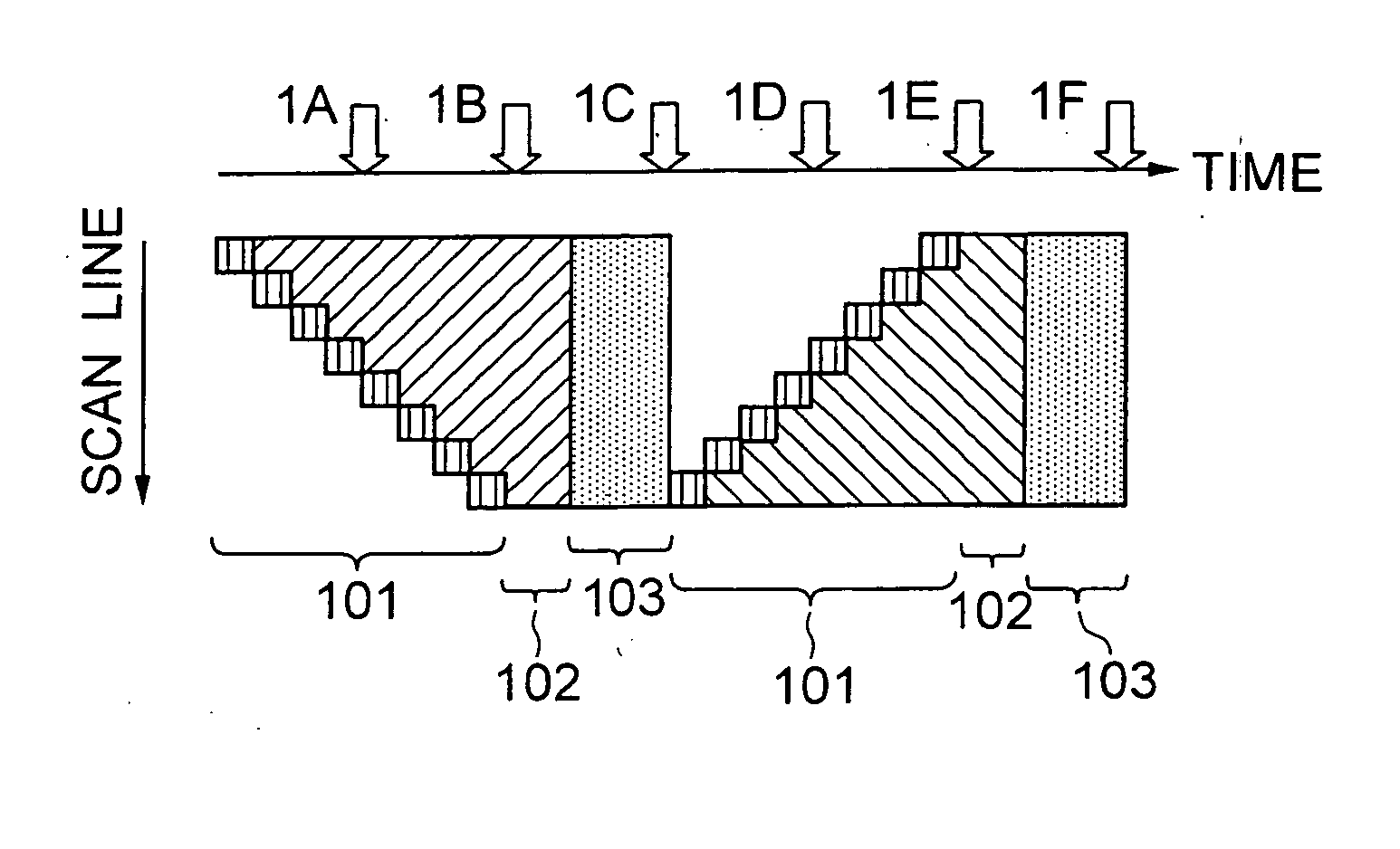
[0095] FIGS. 12(a)-12(c) are time charts that show a second embodiment of the present invention in the same manner as in FIGS. 10(a)-10(c). In the present embodiment, bi-directional scanning is performed as in the first embodiment. However, the present embodiment differs from the first embodiment in that the position of the reset period is changed from that in the first embodiment, and interlace drive is employed. In the present embodiment, one half of the eight scan lines (odd-numbered scan lines, hereinafter called “odd scan lines”) are scanned (selected) in the first field, and the remaining half of the eight scan lines (even-numbered scan lines, hereinafter called “even scan lines”) are scanned (selected) in the second field. The reset period 103 for each scan line is positioned at the end of the field in which the scan line is not scanned (selected). Specifically, for odd scan lines, a write period 101 is provided in the first field such that these scan lines are successively s...

third embodiment

[0099] FIGS. 14(a)-14(c) are time charts that show a third embodiment of the present invention in the same manner as in FIGS. 10(a)-10(c). In the present embodiment, bi-directional scanning is performed in combination with interlace drive as in the second embodiment. The method for driving of the present embodiment can be achieved through modification of the method for driving of the second embodiment such that the frame frequency is doubled. That is, as shown in FIG. 10(a), for odd scan lines, a write period 101 is provided in a first half of the first field such that these scan lines are successively scanned from the top for write operation, followed by a display period 102. A reset period 103 is provided at the end of the first field. The second field is similarly divided into these periods. By contrast, for even scan lines, a reset period 103 is provided at the end of the first half of the first field, a write period 101 is provided in the second half of the first field such tha...

fourth embodiment

[0102] FIGS. 16(a)-16(c) are time charts that show a fourth embodiment in the same manner as in FIGS. 10(a)-10(c). In the present embodiment, bi-directional scanning is performed in combination with interlace drive as in the second and third embodiments. However, the present embodiment differs from the second and third embodiments in that the interlace drive is performed within each of the first and second fields, but the scanning direction in the second field is opposite to that in the first field. That is, for odd scan lines, a write period 101 is provided in a first half of the first field such that these scan lines are successively scanned from the top, followed by a display period 102, and a reset period 103 is provided at the end of the first field. Subsequently, a write period 101 is provided in a first half of the second field such that these scan lines are successively scanned from the bottom, followed by a display period 102, and a reset period 103 is provided at the end o...


PUM

PropertyMeasurementUnit
timeaaaaaaaaaa
timeaaaaaaaaaa
time periodaaaaaaaaaa

Abstract

In a method for driving a liquid crystal display apparatus in which in each field, scan lines are successively scanned in order to display an image, the scanning sequence or the polarity of a signal voltage is reversed between a first field and a second field. A liquid crystal display apparatus driven by the method is also disclosed. It is possible to provide a high contrast, high brightness liquid crystal display apparatus which is not affected by electrical asymmetry.

Description

BACKGROUND OF THE INVENTION [0001] (a) Field of the Invention [0002] The present invention relates to a liquid crystal display apparatus and a method of driving the same, and more particularly to a method of driving a liquid crystal display element which provides high contrast and high brightness and which is not affected by electrical asymmetry, as well as a liquid crystal display apparatus having a liquid crystal display element that is driven by such a method. [0003] (b) Description of the Related Art [0004] The mainstream of a high performance liquid crystal display apparatus is a TFT (thin-film transistor)-scheme active matrix liquid crystal display apparatus of a TN (twisted nematic) mode using nematic liquid crystal or an IPS (in-plane switching) mode. In such an active matrix liquid crystal display apparatus, an image is re-displayed at 60 Hz, because positive and negative image signals are written at 30 Hz, making the time period of one field about 16.7 ms (millisecond). Th...

Claims


Application Information

Patent Timeline
Patent Type & Authority Applications(United States)
IPC IPC(8): G02F1/133G09G3/20G09G3/36G09G5/00
CPCG09G3/2025G09G3/3611G09G3/3614G09G2310/0283G09G2320/0247G09G2320/0204G09G2320/0223G09G2320/0233G09G2310/061
Inventor TAKATORI, KENI-ICHISUMIYOSHI, KENUEHARA, SHIN-ICHI
Owner NEC LCD TECH CORP
Why Eureka
Try Eureka