Method for manufacturing LCD device with integrated touch panel

a technology of touch panel and lcd device, which is applied in the direction of electric digital data processing, instruments, computing, etc., can solve the problems of impracticality of installing near field images (nfi), the area of such driving circuits becomes even larger, and the effect of reducing the volume and weight of lcd devices

Inactive Publication Date: 2005-10-20
INNOLUX CORP
View PDF3 Cites 124 Cited by
  • Summary
  • Abstract
  • Description
  • Claims
  • Application Information

AI Technical Summary

Benefits of technology

[0010] It is a further object of this invention to decrease the whole volume and weight of the LCD device with touch panel. An LCD panel having a common substrate is provided. Then, a touch panel is formed on the common substrate.

Problems solved by technology

Due to the poor accuracy of the screen printing method, the area of such driving circuit becomes larger.
Besides, when a complicated driving circuit, such as near field image (NFI) type or capacitive type, of a touch panel is required, the dri

Method used


Image

  • Method for manufacturing LCD device with integrated touch panel
  • Method for manufacturing LCD device with integrated touch panel
  • Method for manufacturing LCD device with integrated touch panel

Examples


Embodiment Construction

[0017] Some sample embodiments of the present invention will now be described in greater detail. Nevertheless, it should be recognized that the present invention can be practiced in a wide range of other embodiments besides those explicitly described, and the scope of the present invention is expressly not limited except as specified in the accompanying claims.

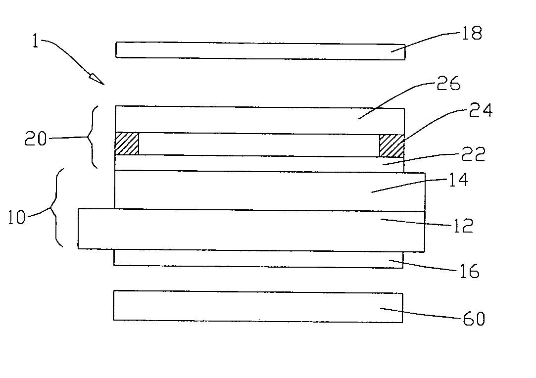
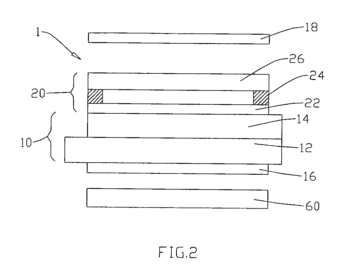
[0018]FIG. 2 shows a cross-sectional view of a liquid crystal display (LCD) device 1 with an integrated touch panel according to an embodiment of the present invention is shown. The LCD device 1 includes an LCD panel 10, a touch panel 20, a first polarizer 16, a second polarizer 18, and a light source 60. The first polarizer 16 is located between the LCD panel 10 and the light source 60, and the second polarizer 18 is located on the touch panel 20. The LCD panel 10 has a lower substrate 12 and a common substrate 14. A TFT array (not shown in the figure) is on the lower substrate 12 for controlling the direction of liquid crys...


PUM


Abstract

A driving circuit of a touch panel is formed by the photolithographic process on the liquid crystal display (LCD) panel to reduce the area of the driving circuit. The method includes providing an LCD panel having a common substrate; and forming a touch panel on the common substrate. First, a first conducting layer is formed on the common substrate, and then a second patterned conducting layer is formed on the first conducting layer and on a peripheral region of the LCD panel by a photolithographic process. The common substrate of the LCD panel is used as an upper substrate of the LCD panel and as a lower substrate for the touch panel.

Description

BACKGROUND OF THE INVENTION [0001] 1. Field of the Invention [0002] The invention relates to a method for manufacturing LCD device with integrated touch panel, more particularly to a method for manufacturing LCD device with integrated touch panel to form driving circuit of touch panel onto the LCD panel by photolithographic process. [0003] 2. Description of the Prior Art [0004] A touch panel can read the operation of the user by coordinate values and input data. A touch panel is usually installed onto a flat display device such as a thin film transistor (TFT) display device. For example, the Automatic Teller Machines (ATM) with touch panel are located in the bank or along the roadside. When a touch pen or a fingertip presses on the surface of touch panel, a potential signal will be generated in the corresponding point. The information represented from such signal can be processed by other devices. [0005] Please refer to FIG. 1, an LCD device 100 including a LCD panel 110 and a touch...

Claims


Application Information

Patent Timeline
IPC IPC(8): G09G3/36
CPCG02F1/13338
Inventor MING, JHENG CI
Owner INNOLUX CORP
Why Eureka
Try Eureka