
Flash memory device capable of preventing an over-erase of flash memory cells and erase method thereof

a flash memory and over-erasing technology, applied in static storage, digital storage, instruments, etc., can solve the problems of increasing the overall time it takes to erase the memory cell, the length of time that it takes to perform the additional erase repair operation, etc., to reduce the total erase operation time and erase method, and minimize the number of flash memory cells over-erased

Inactive Publication Date: 2005-10-20
SAMSUNG ELECTRONICS CO LTD
View PDF37 Cites 2 Cited by
  • Summary
  • Abstract
  • Description
  • Claims
  • Application Information

AI Technical Summary

Benefits of technology

The present invention provides a flash memory device and method for erasing memory cells that reduces the total erase operation time and minimizes the number of flash memory cells over-erased during an erase operation. The method includes applying a first electric field during a first interval and step-wise incrementing it, and applying a second electric field during a second interval and maintaining constant it. The device includes a sense amplifier circuit, a high voltage generating circuit, an erase controller, and a row and column selecting circuit. The erase controller checks if a threshold voltage of at least one cell reaches a verify voltage over a maximum value of a target threshold voltage range corresponding to an erased state, and controls the high voltage generating circuit to step-wise increase the bulk voltage generated therefrom when the threshold voltage of the cell reaches the verify voltage. The device also includes a row counter and a column counter for generating the row and column addresses.

Problems solved by technology

One problem associated with the above-described erase method is the length of time that it takes to perform the additional erase repair operation.
This is because the repair operation increases the overall time it takes to erase the memory cell.
As well known to those skilled in the art, such a problem arises when excess electric field is applied across the floating gate of the flash memory cell.

Method used


Image

  • Flash memory device capable of preventing an over-erase of flash memory cells and erase method thereof
  • Flash memory device capable of preventing an over-erase of flash memory cells and erase method thereof
  • Flash memory device capable of preventing an over-erase of flash memory cells and erase method thereof

Examples


Embodiment Construction

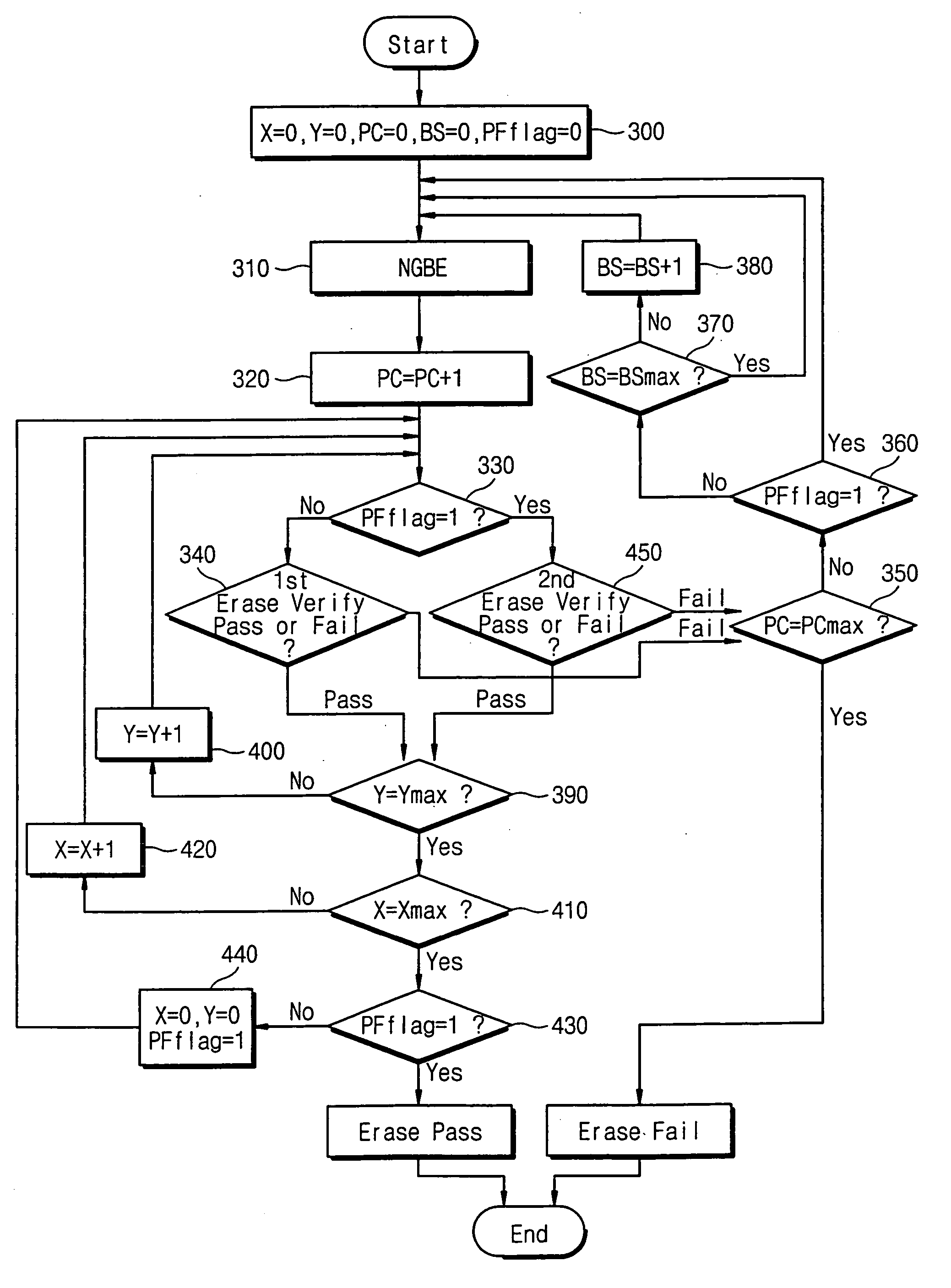
[0038] The preferred embodiment of the invention will be more fully described with reference to the attached drawings.

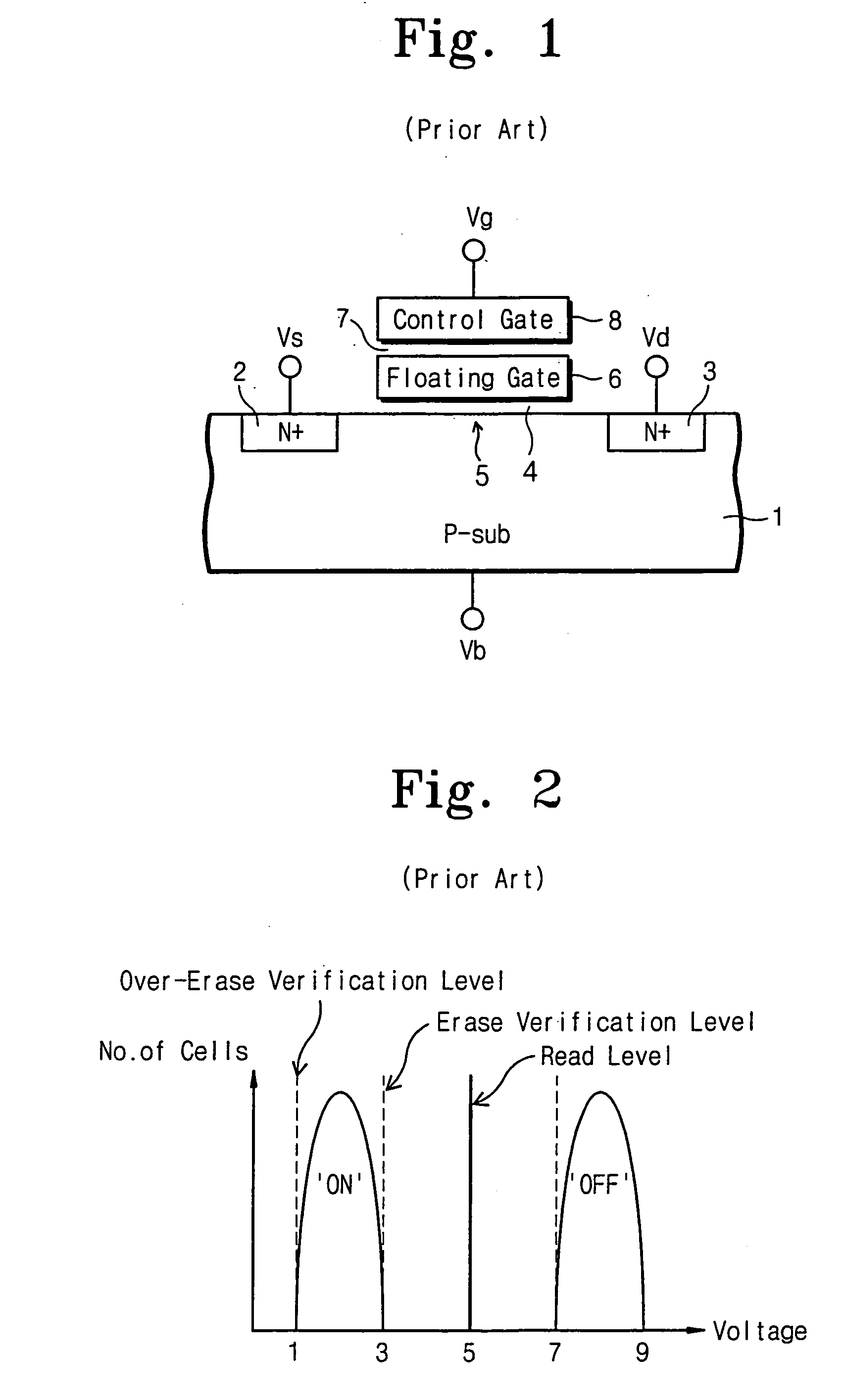
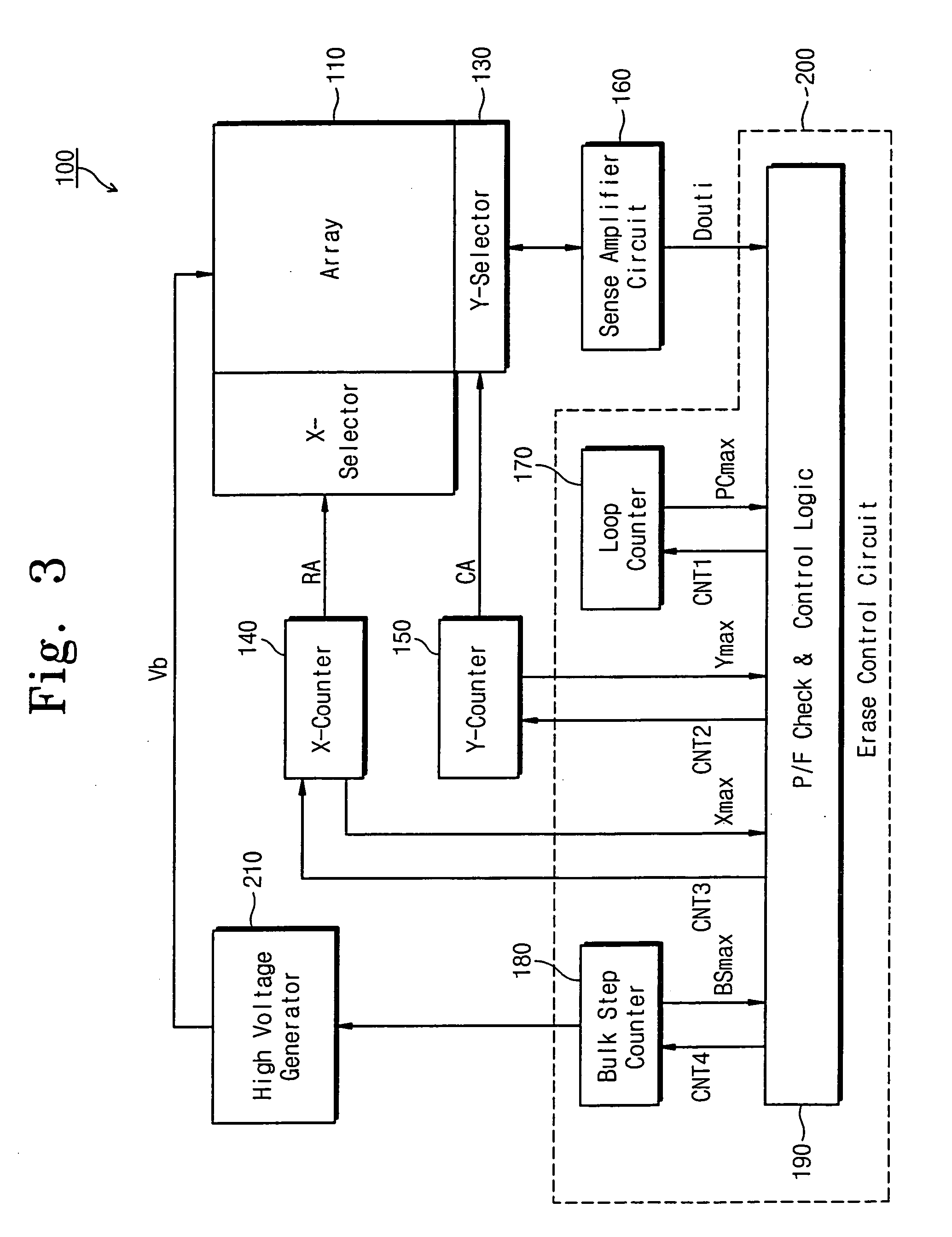
[0039] Referring to FIG. 3, a flash memory device is illustrated in block form. The flash memory device 100 includes an array 110 of flash memory cells having the same structure as illustrated in FIG. 1. The flash memory cells are arranged in a matrix of rows and columns. Although not illustrated in the drawing, it should readily apparent to a person of skill in the art that a plurality of word lines and a plurality of bit lines extend along the rows and the columns, respectively. The flash memory cells in the array 110 are formed on a single bulk or substrate such that they are simultaneously erased. The cell array 110 shown in FIG. 3 corresponds to a sector or a block. A NOR-type flash memory device having a sector or block architecture is disclosed in A 3.3V-only 16 Mb Flash Memory with Row-Decoding Scheme by Kang-Deog Suh, IEEE International Solid-State Circuits...


PUM


Abstract

The flash memory device according to the present invention includes an erase control circuit, used as a state machine, having embodied erase algorithm which can prevent flash memory cells from being over-erased. The erase control circuit, first, checks whether or not threshold voltages of selected cells reach a predetermined pre-verify voltage higher than the maximum value of a target threshold voltage range corresponding to the erased state. When at least one of the selected cells has its threshold voltage higher than the pre-verify voltage, a high voltage generator generates a bulk voltage that is increased step by step by a predetermined voltage level. And, when the selected cells all have threshold voltages equal to or less than the pre-verify voltage, the high voltage generator generates a constant bulk voltage. According to this bulk voltage control scheme, the number of flash memory cells over-erased at the erase operation is reduced reducing the total erase time.

Description

[0001] This application is a continuation of U.S. patent application Ser. No. 10 / 430,364, filed May 5, 2003, now pending, which is a continuation-in-part of U.S. patent application Ser. No. 10 / 016,579, now issued U.S. Pat. No. 6,577,540, which is a divisional of U.S. patent application Ser. No. 09 / 626,172, now issued U.S. Pat. No. 6,314,027, which claims priority from Korean Patent Application No. 1999-30872, filed on Jul. 28, 1999, all of which are hereby incorporated by reference in their entirety.FIELD OF THE INVENTION [0002] The present invention relates generally to nonvolatile memory devices and, more particularly, to a flash memory device capable of preventing flash memory cells from being over-erased and an erase method thereof. BACKGROUND OF THE INVENTION [0003] Nonvolatile memory devices have become increasingly popular, especially flash memory devices. FIG. 1 shows a conventional flash memory cell. The flash memory cell has source and drain regions 2 and 3, respectively, ...

Claims


Application Information

Patent Timeline
Patent Type & Authority Applications(United States)
IPC IPC(8): G11C11/34G11C16/34
CPCG11C16/3418G11C16/3477G11C16/3468
Inventor CHOI, KI-HWAN
Owner SAMSUNG ELECTRONICS CO LTD
Learn More