

Magnetic random access memory and operation method thereof
a random access memory and magnetic technology, applied in the direction of information storage, static storage, digital storage, etc., can solve the problems of shortened write time and increase the probability of erroneous writing, and achieve the effect of reducing power consumption and an operation method thereo
- Summary
- Abstract
- Description
- Claims
- Application Information
AI Technical Summary
Benefits of technology
Problems solved by technology
Method used
Image

Examples
first embodiment
1. FIRST EMBODIMENT
1-1. Circuit Configuration
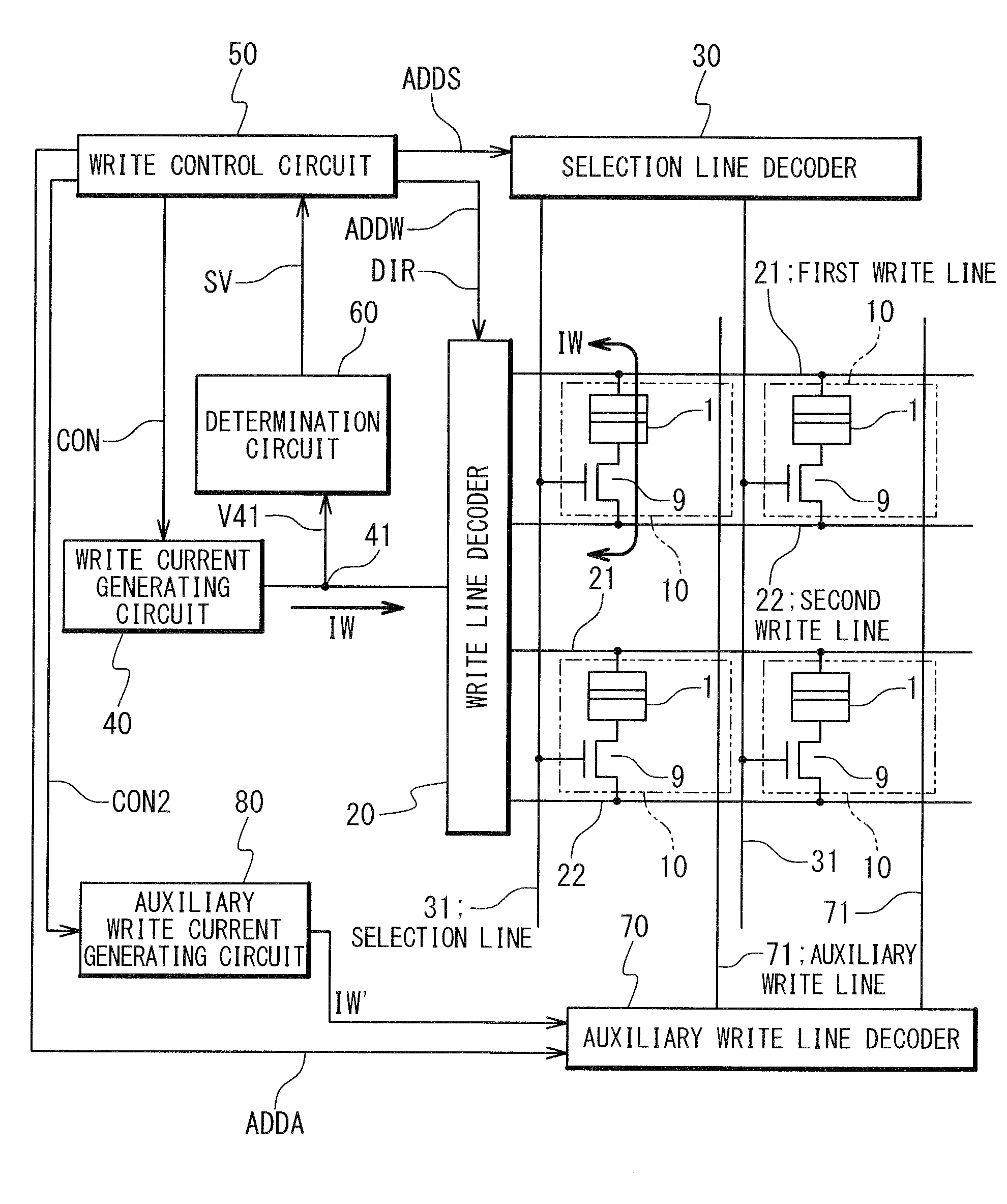
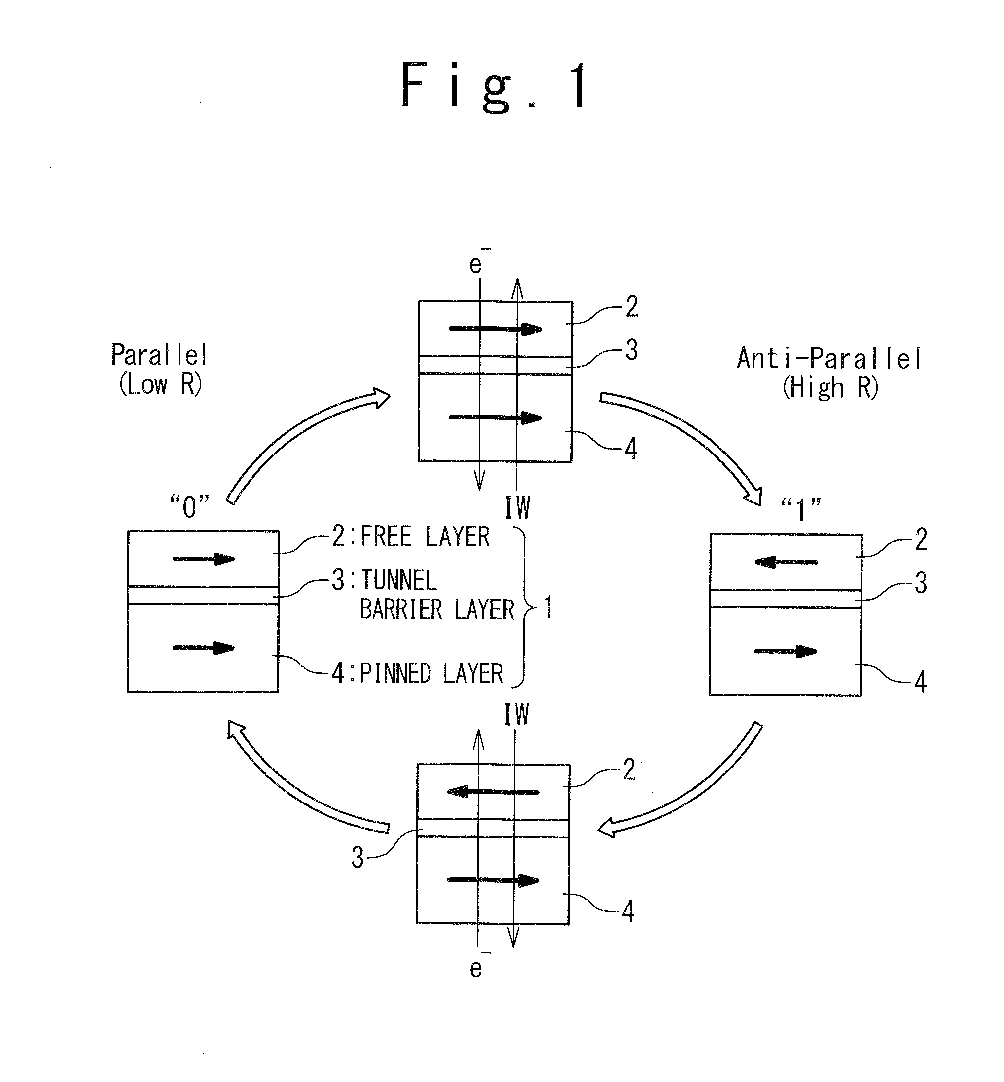
[0064]FIG. 3 is a circuit block diagram showing a configuration of a MRAM of a first embodiment according to the present invention. The MRAM includes a memory cell array including a plurality of memory cells 10 arranged in a matrix form. Each of the memory cells 10 includes a magnetoresistance element 1 shown in FIG. 1 and a selection transistor 9. As shown in FIG. 1, the magnetoresistance element 1 includes a free layer 2, a tunnel barrier 3, and a pinned layer 4. The pinned layer 4 whose magnetization orientation is fixed is formed to be thicker than the free layer 2, serving as a mechanism (a spin filter) to create a spin-polarized current. The desired data is written into the memory cell 10 by the write current IW that is vertically transferred into film planes of the magnetoresistance elements 1. A direction of the write current IW is determined by being dependent on desired data to be written.
[0065]One end of the magnetoresistance e...
second embodiment
2. SECOND EMBODIMENT
2-1. Circuit configuration
[0096]FIG. 8 is a circuit block diagram showing a configuration of the MRAM of a second embodiment according to the present invention. In FIG. 8, the same reference letters as those of FIG. 3 refer to the same elements as those of FIG. 3, and explanation thereof will be appropriately omitted. In the present embodiment, the determination circuit 60 includes a calculation comparator 62. The electrical potential V41 and a current signal SI indicating a value of the write current IW are inputted to the calculation comparator 62. The calculation comparator 62 then calculates a “ratio” between the electrical potential V41 and the write current IW, and compares the “ratio” with a predetermined reference value. The “ratio” exhibits a value obtained by dividing the electrical current V41 by the write current IW, or a value obtained by dividing the write current IW by the electrical potential V41.
[0097]The reason why the calculation comparator 62 ...
third embodiment
3. THIRD EMBODIMENT
3-1. Circuit Configuration
[0112]FIG. 14 is a circuit block diagram showing a configuration of the MRAM of a third embodiment according to the present invention. In FIG. 14, the same reference letters as those of FIG. 3 refer to the same elements as those of FIG. 3, and explanation thereof will be appropriately omitted. In the present embodiment, the determination circuit 60 includes a potential monitor 63 for monitoring the electrical potential V41 of the node 41.
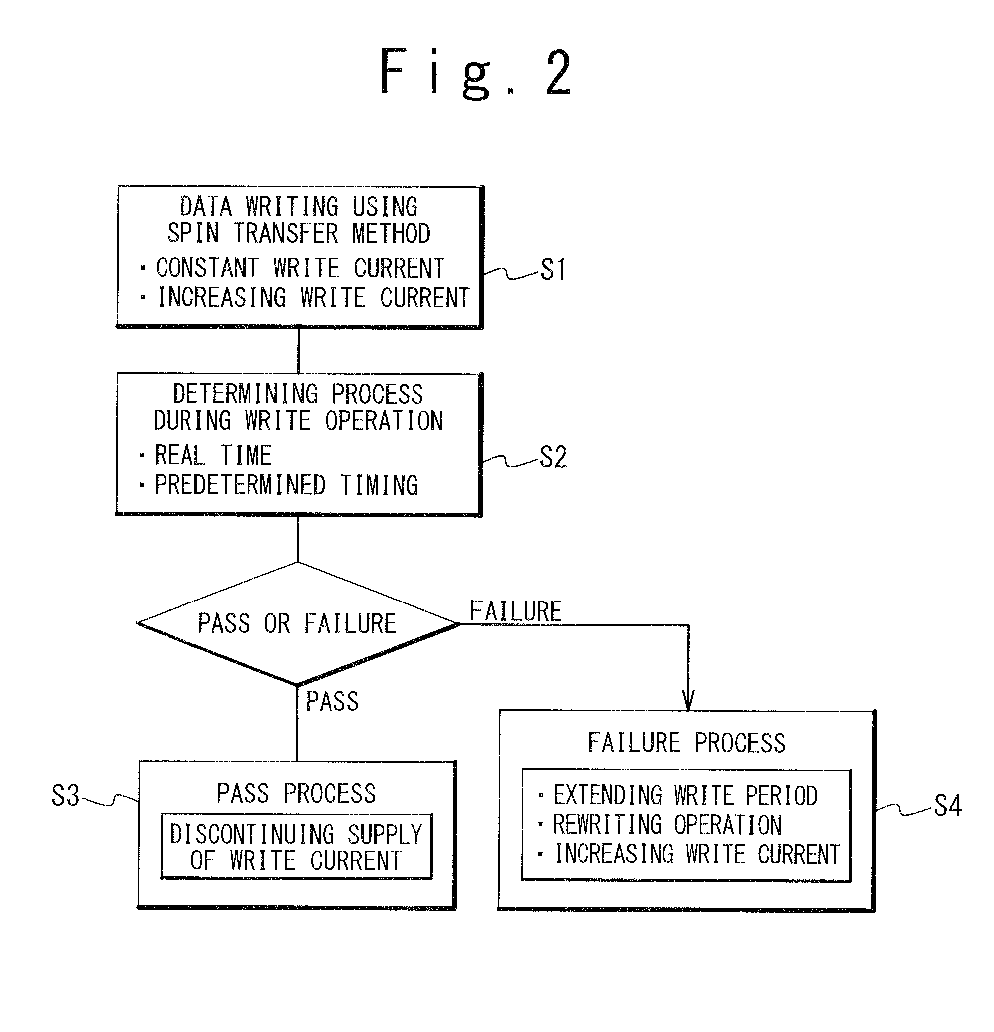
[0113]The determination circuit 60 may not necessarily carry out the aforementioned determination in real time. The write control circuit 50 outputs a verifying instruction signal VER to the potential monitor 63 at a predetermined timing during the write period PW. The potential monitor 63 determines whether or not desired data is written at the predetermined timing on the basis of the electrical potential V41 (or information on the electrical potential V41). The potential monitor 63 then outputs a verify...
PUM
 Abstract
Description
Claims
Application Information