Nonlithographic method to produce self-aligned mask, articles produced by same and compositions for same

a non-lithographic method and mask technology, applied in the direction of circuit masks, instruments, photomechanical equipment, etc., can solve the problems of reducing the effective dielectric constant of typical procedures used to generate masks by lithographic or other means, so as to achieve simple and robust effects

Inactive Publication Date: 2005-10-20
GLOBALFOUNDRIES INC
View PDF17 Cites 12 Cited by
  • Summary
  • Abstract
  • Description
  • Claims
  • Application Information

AI Technical Summary

Benefits of technology

[0005] This invention relates to a method to fabricate mask layers onto a pre-patterned substrate having two or more chemically distinct surface regions, or two or more surface regions that have undergone different surface treatment. The mask layer is deposited by a self-assembly approach that provides self-alignment of the layers. This method can apply to any technology or application involving a chemically or physically heterogeneous substrate including: interconnect structures for high speed microprocessors, application specific integrated circuits (ASICs), flexible organic semiconductor chips, and memory storage. Other structures that can be fabricated utilizing this method include: displays, circuit boards, chip carriers, microelectromechanical systems (MEMS), chips for hi-thoughput screening, microfabricated fluidic devices, etc. The utility of this method stems from a simple and robust means in which the replication of a patterned substrate to generate a mask layer can be performed, circumventing the requirement for difficult and error prone methods, such as lithography. Thus, the present invention provides an extremely advantageous alternative to the prior art techniques.
[0007] Thus, in the example of integrated circuits, the use of the self-aligned masks allows a simplified fabrication process in which the effective dielectric constant between metal lines can be reduced through selective application of various materials to the metal lines. This is of great importance in maximizing the propagation speed of interconnect signals and ultimately provides faster overall circuit performance. Furthermore, the present invention leads to a higher level of protection and reliability of interconnect structures and to reduced processing costs.
[0008] Another application of this invention is its use for semiconductor packaging substrates which are comprised of conductors (usually copper) and insulators (usually epoxy, polyimide, alumina, cordierite glass ceramic and the like) disposed adjacent to each other. The conductors can be protected from external ambients, and process exposures such as soldering and wet etching. This protection can be achieved by using the various methods of forming selective coatings on the conductor. Alternately, selective coating on the dielectric by one of the exemplary methods can leave the metal exposed for further processing by methods such as electroless plating to add additional metal layers such as nickel, cobalt, palladium, gold and others, on top, without exposing the dielectrics to these process steps.
[0009] The ability to accomplish these selective modifications without the use of lithographic processing leads to cost reductions and is particularly advantageous in microelectronic packaging which is very cost sensitive.

Problems solved by technology

Unfortunately, typical procedures used to generate a mask by lithographic or other means can be expensive and error prone.
Both of these approaches reduce the effective dielectric constant, keff, of the components between metal lines and as a result, interconnect signals travel faster through conductors due to a reduction in resistance-capacitance (RC) delays.
Unfortunately, these strategies are difficult to implement due to limitations in maintaining sufficient properties, i.e., mechanical, barrier, electrical, etc., that result with a reduction in thickness or a change in the chemistry of the layers.

Method used


Image

  • Nonlithographic method to produce self-aligned mask, articles produced by same and compositions for same
  • Nonlithographic method to produce self-aligned mask, articles produced by same and compositions for same
  • Nonlithographic method to produce self-aligned mask, articles produced by same and compositions for same

Examples


Embodiment Construction

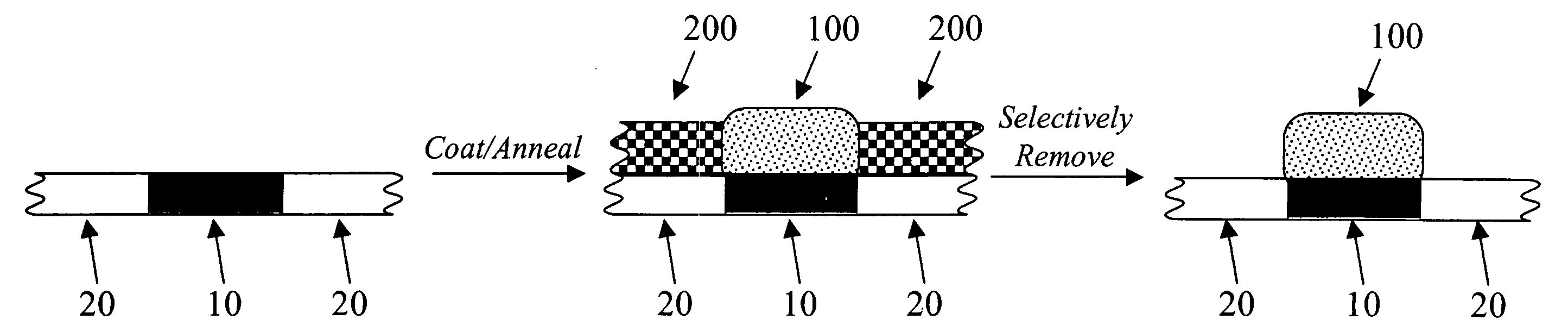
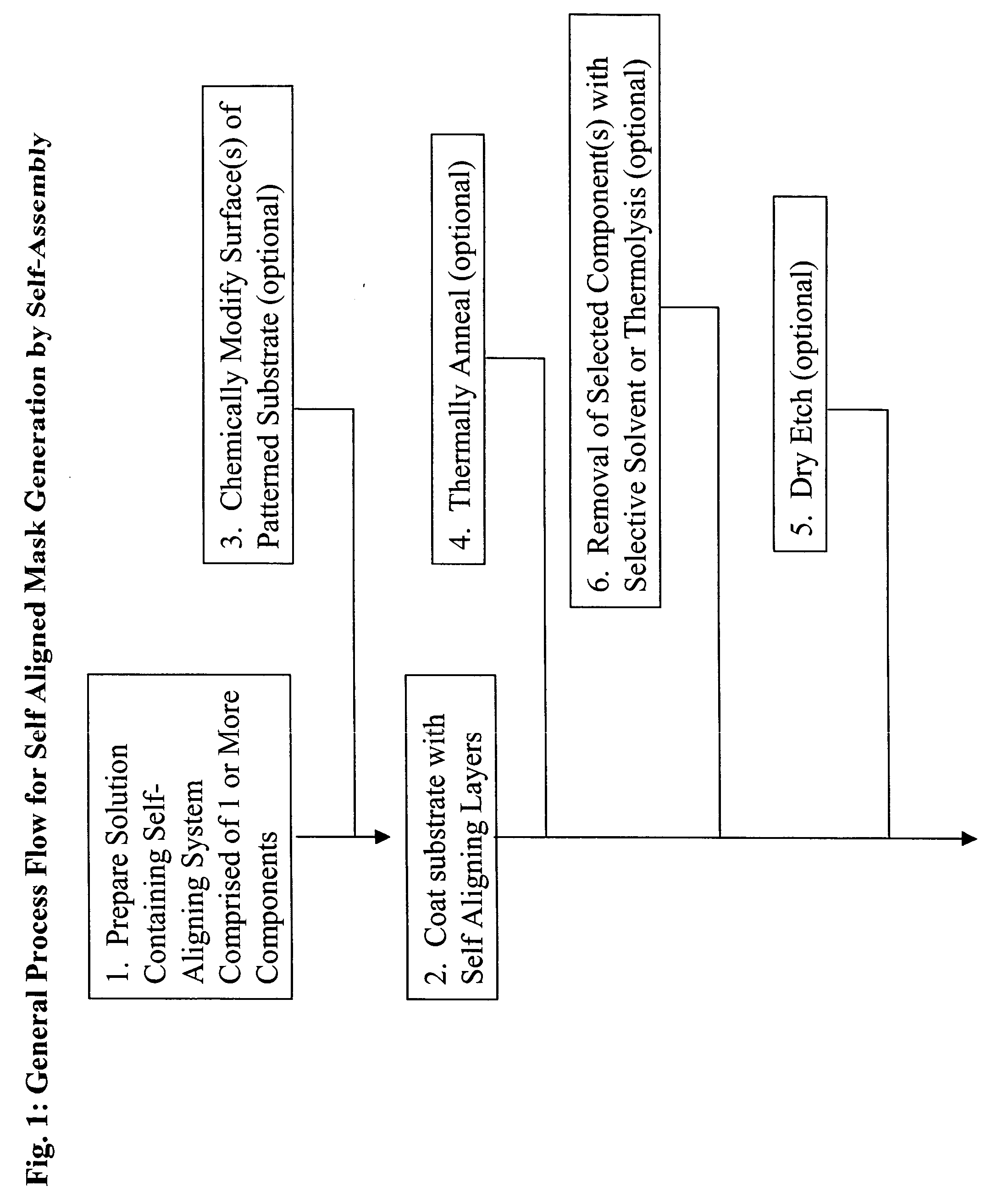
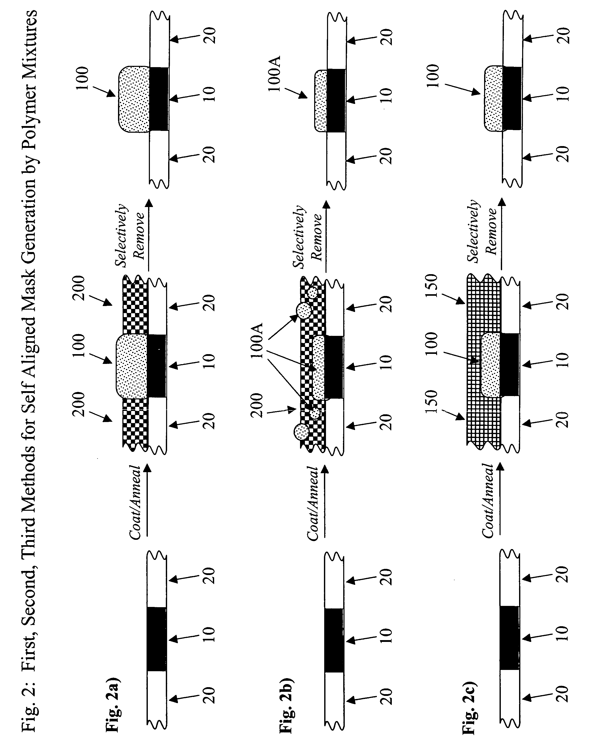
[0033] In accordance with the invention, a patterned substrate containing structures having two or more distinct components is processed by a route whereby layers can be applied to selected component surfaces. This layer can be generated by a number of self-assembly approaches described below and can be used as a mask layer for subsequent treatment or material deposition onto the intended component surfaces. These structures can be sacrificial and, in general, do not remain in the final structure. The use of the masks for the generation of self assembled barrier layers can proceed by a number of routes including: blanket deposition followed by lift-off, blanket deposition followed by chemical mechanical polishing (CMP), and enhancement of selective electrochemical and electroless metal deposition processes. It will be clear to one skilled in the art that the application of a self-aligned layer by any of the approaches described below can be used as a process to generate a selective ...


PUM

PropertyMeasurementUnit
length scalesaaaaaaaaaa
dielectric constantsaaaaaaaaaa
compositionaaaaaaaaaa

Abstract

A method for forming a self aligned pattern on an existing pattern on a substrate comprising applying a coating of a solution containing a masking material in a carrier, the masking material having an affinity for portions of the existing pattern; and allowing at least a portion of the masking material to preferentially assemble to the portions of the existing pattern. The pattern may be comprised of a first set of regions of the substrate having a first atomic composition and a second set of regions of the substrate having a second atomic composition different from the first composition. The first set of regions may include one or more metal elements and the second set of regions may include a dielectric. The first and second regions may be treated to have different surface properties. Structures made in accordance with the method. Compositions useful for practicing the method.

Description

CROSS REFERENCE TO RELATED APPLICATION [0001] This application is related to the application entitled “Nonlithographic Method to Produce Mask by Selective Reaction, Articles Produced, and Compositions for Same” (docket number YOR920020155US1) by the same inventors as the present invention, filed on the same day as the present application, and assigned to the same assignee as the present application and which is incorporated herein by reference as if fully set forth herein. FIELD OF THE INVENTION [0002] This invention relates to the production of patterns on a substrate having regions with different compositions or different surface treatment. More particularly, it relates to a method of producing fine patterns on substrates used in, for example, the microelectronics industry on which electronic devices are fabricated. It is also related to devices fabricated in accordance with the methods. The patterns are fabricated accurately and inexpensively without the use of lithography. The p...

Claims


Application Information

Patent Timeline
Patent Type & Authority Applications(United States)
IPC IPC(8): H01L21/027B32B3/00G03F7/00G03F7/16G03F7/26H01L21/31H01L21/3105H01L21/469
CPCH01L21/0331H01L21/76849Y10T428/24802H05K3/282H05K2203/1173H05K3/0079H01L21/027
Inventor COLBURN, MATTHEW E.GATES, STEPHEN M.HEDRICK, JEFFREY C.HUANG, ELBERTNITTA, SATYANARAYANA V.PURUSHOTHAMAN, SAMPATHSANKARAPANDIAN, MUTHUMANICKAM
Owner GLOBALFOUNDRIES INC
Why Eureka
Try Eureka