

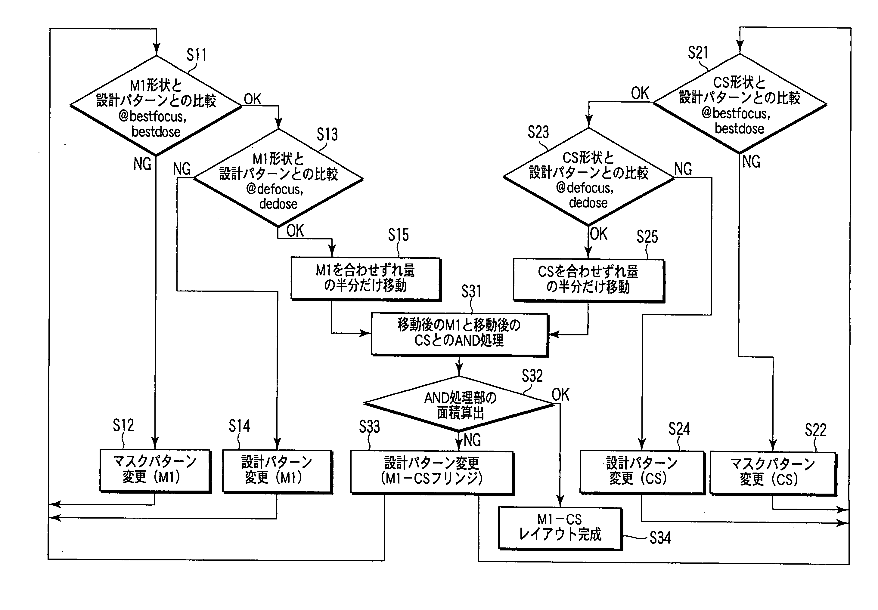
Design pattern correction method and mask pattern producing method
a mask pattern and correction method technology, applied in the field of design pattern correction methods, can solve the problems of insufficient detection accuracy, inability to faithfully form a pattern in individual processes, and inability to provide the final processed pattern shap
- Summary
- Abstract
- Description
- Claims
- Application Information
AI Technical Summary
Benefits of technology
Problems solved by technology
Method used
Image

Examples
first embodiment
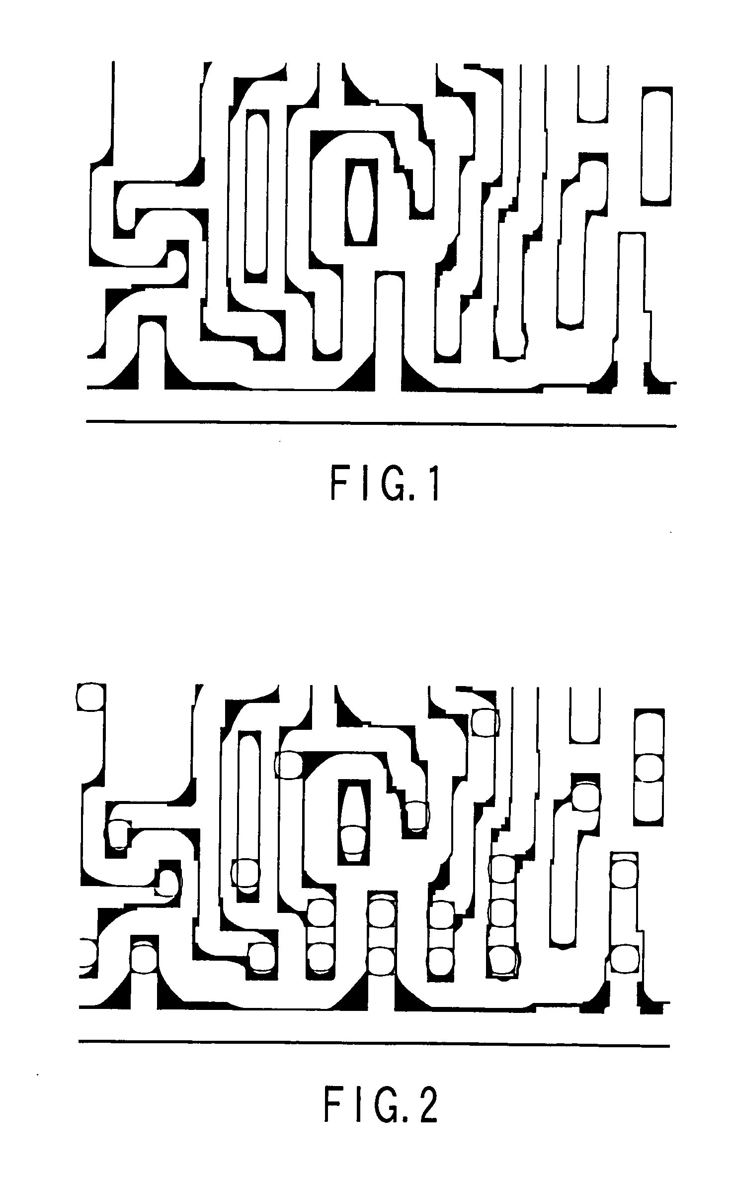
[0032]FIG. 1 is a view showing the result when OPC is made with respect to a single layer. In this case, a metal interconnect (M1) layer is assumed. In FIG. 1, portions painted with black show deviations from a design pattern (target pattern) of the pattern after OPC.
[0033]FIG. 2 is a view showing the result when OPC is made with respect to several layers. A metal interconnect (M1) is assumed as a first layer based on a first design pattern. A contact hole (CS) is assumed as a second layer based on a second design pattern. The best condition is given with respect to exposure dose and focal position. In FIG. 2, an overlay error between M1 and CS is not considered.
[0034] An AND region of a processed pattern shape of the M1 and that of the CS require a predetermined area or more. For example, the area of an AND region of the design pattern of the M1 and that of the CS is set as A1. In addition, the area of the AND region of the processed pattern shape of the M1 and that of the CS is ...
second embodiment
[0067] The second embodiment of the present invention will be described below.
[0068] In FIG. 8, an assumption is given such that the alignment error a uniformly distributes; however, in fact, the alignment error (a) depends on a probability distribution. FIG. 10 shows one example when the probability distribution of the alignment error is a normal distribution, and 3σ is set as b.
[0069] The probability distribution of the alignment error is a normal distribution of 3σ=b; therefore, a probability distribution shown in FIG. 10 (2) is given. The area of the AND region of ring pattern and metal pattern in each alignment error position is calculated according to the method shown in FIG. 8 and FIG. 9. When an area calculated in each alignment error position is taken as the vertical axis, an area distribution shown in FIG. 10 (3) is given. Convolution integral of the probability distribution (2) and the area (3) is made. By doing so, an effective area distribution (4) of the AND region o...
third embodiment
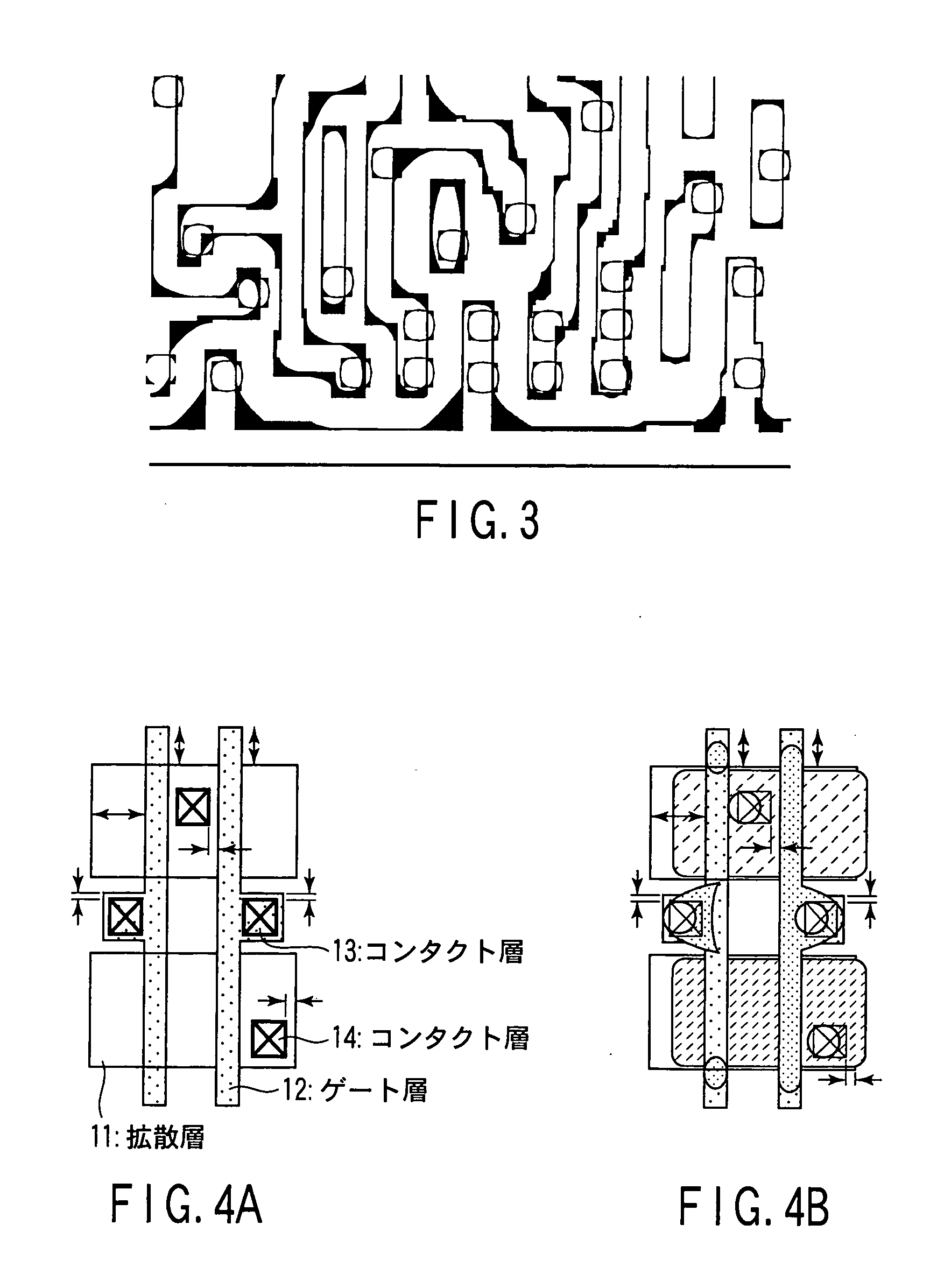
[0077]FIG. 11A, FIG. 11B, FIG. 12A and FIG. 12B are views to explain a third embodiment of the present invention. FIG. 11A and FIG. 12A each show a design layout, and FIG. 11B and FIG. 12B each show a processed pattern shape on a wafer. In FIG. 11A, a reference numeral 11 denotes a diffusion layer, 12 denotes a gate layer, 13 and 14 denote contact layers. In FIG. 12A and FIG. 12B, upper-side views show the case where a distance (a) is short, and lower-side views show the case where the distance (a) is long.
[0078] The embodiment is applicable to evaluation based on each processed shape of gate layer, diffusion layer and contact layer. The criterion for layout corrections of metal layer and contact layer is as follows. That is, the area of the AND region of these layers is used as an index, and it is determined whether or not the area is more than a predetermined value. In particular, a gate line tip portion surrounded with a circle in FIG. 11A has a problem in the gate layer and the...
PUM
| Property | Measurement | Unit |
|---|---|---|
| shape | aaaaa | aaaaa |
| length | aaaaa | aaaaa |
| width | aaaaa | aaaaa |
Abstract
Description
Claims
Application Information