
Top emission organic light emitting diode display using auxiliary electrode to prevent voltage drop of upper electrode and method of fabricating the same

a technology of organic light-emitting diodes and auxiliary electrodes, which is applied in the direction of basic electric elements, electrical apparatus, and semiconductor devices, can solve the problems of non-uniform brightness and image characteristics, increased specific resistance, and deterioration of ito or izo layers, so as to prevent or reduce the voltage drop of upper electrodes.

Inactive Publication Date: 2005-10-27
SAMSUNG DISPLAY CO LTD
View PDF8 Cites 65 Cited by
  • Summary
  • Abstract
  • Description
  • Claims
  • Application Information

AI Technical Summary

Benefits of technology

[0016] The present invention, therefore, solves aforementioned problems associated with conventional displays by providing an organic light emitting diode (OLED) display using an auxiliary electrode to prevent or reduce a voltage drop of an upper electrode.
[0017] In exemplary embodiments of the present invention, a top emission OLED display capable of preventing or reducing a voltage drop of an upper electrode improves brightness and image characteristics such that the top emission OLED display can be large-sized.
[0019] An edge of the auxiliary electrode may have a taper angle of at least 90°. The edge of the auxiliary electrode may have a taper angle between 90° and 135°. The auxiliary electrode may prevent or reduce a voltage drop of the upper electrode.

Problems solved by technology

When the low temperature deposition method is used, however, the quality of the ITO or IZO layer is deteriorated and its specific resistance is increased.
As a result, non-uniformity of brightness and image characteristics may be generated and power consumption may increase.
Also, due to the voltage drop, it is difficult to apply to a middle-sized or large-sized top emission AMOLED display.

Method used


Image

  • Top emission organic light emitting diode display using auxiliary electrode to prevent voltage drop of upper electrode and method of fabricating the same
  • Top emission organic light emitting diode display using auxiliary electrode to prevent voltage drop of upper electrode and method of fabricating the same
  • Top emission organic light emitting diode display using auxiliary electrode to prevent voltage drop of upper electrode and method of fabricating the same

Examples


Embodiment Construction

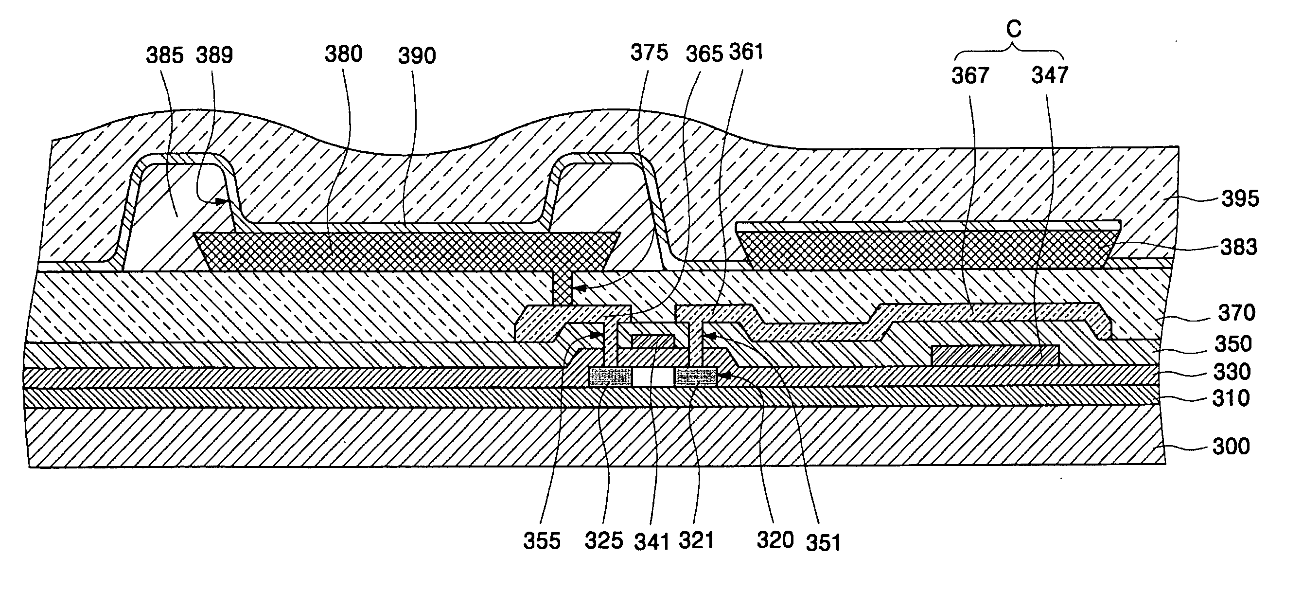
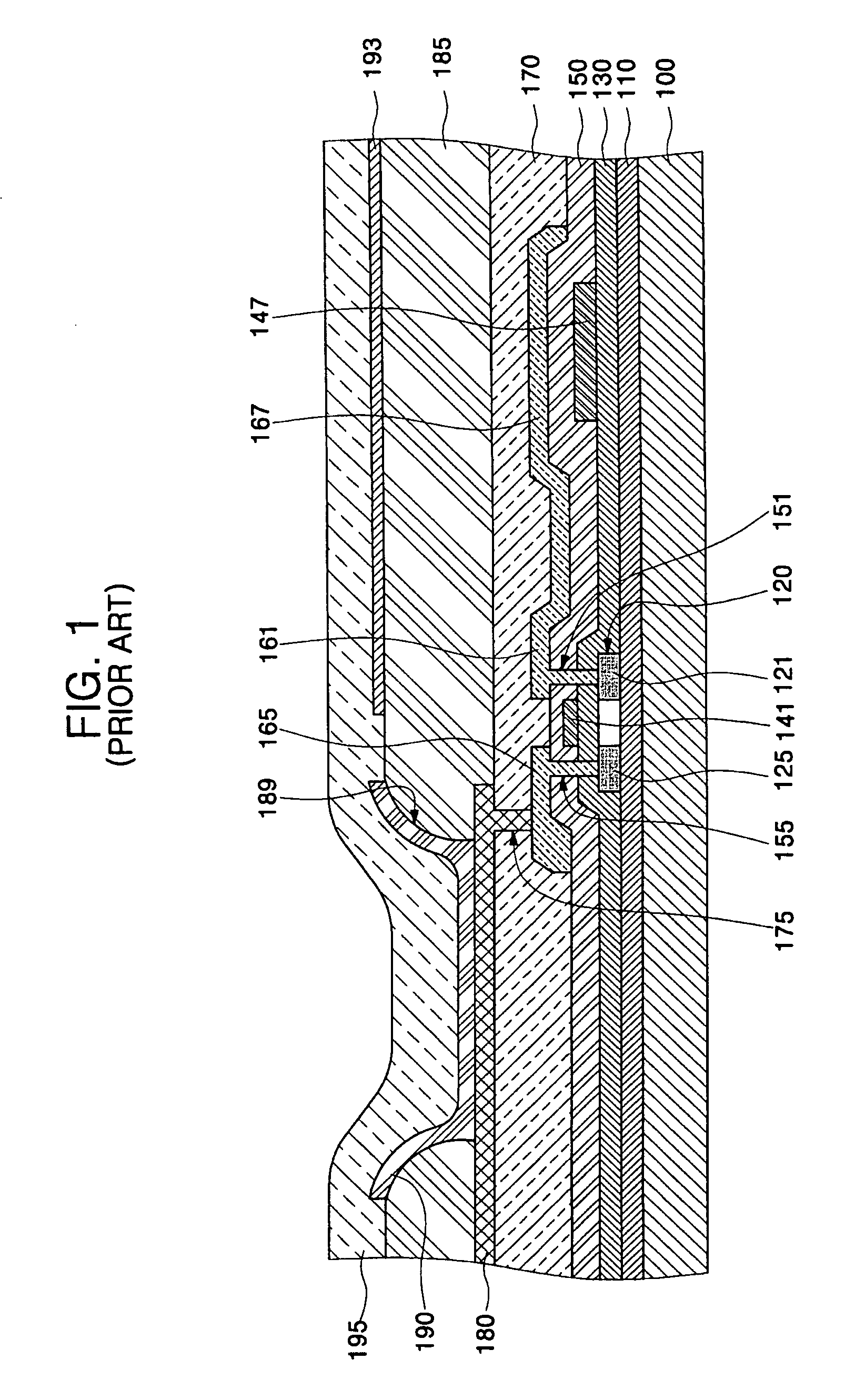
[0039] The present invention will now be described more fully hereinafter with reference to the accompanying drawings, in which certain exemplary embodiments of the invention are shown. This invention may, however, be embodied in different forms and should not be construed as limited to the embodiments set forth herein. Like reference numerals refer to like elements throughout the specification. Also, when a layer is described as being formed on a substrate in this specification, the layer may be formed directly on the substrate, or it may be formed on the substrate with one or more other layers that are formed therebetween.

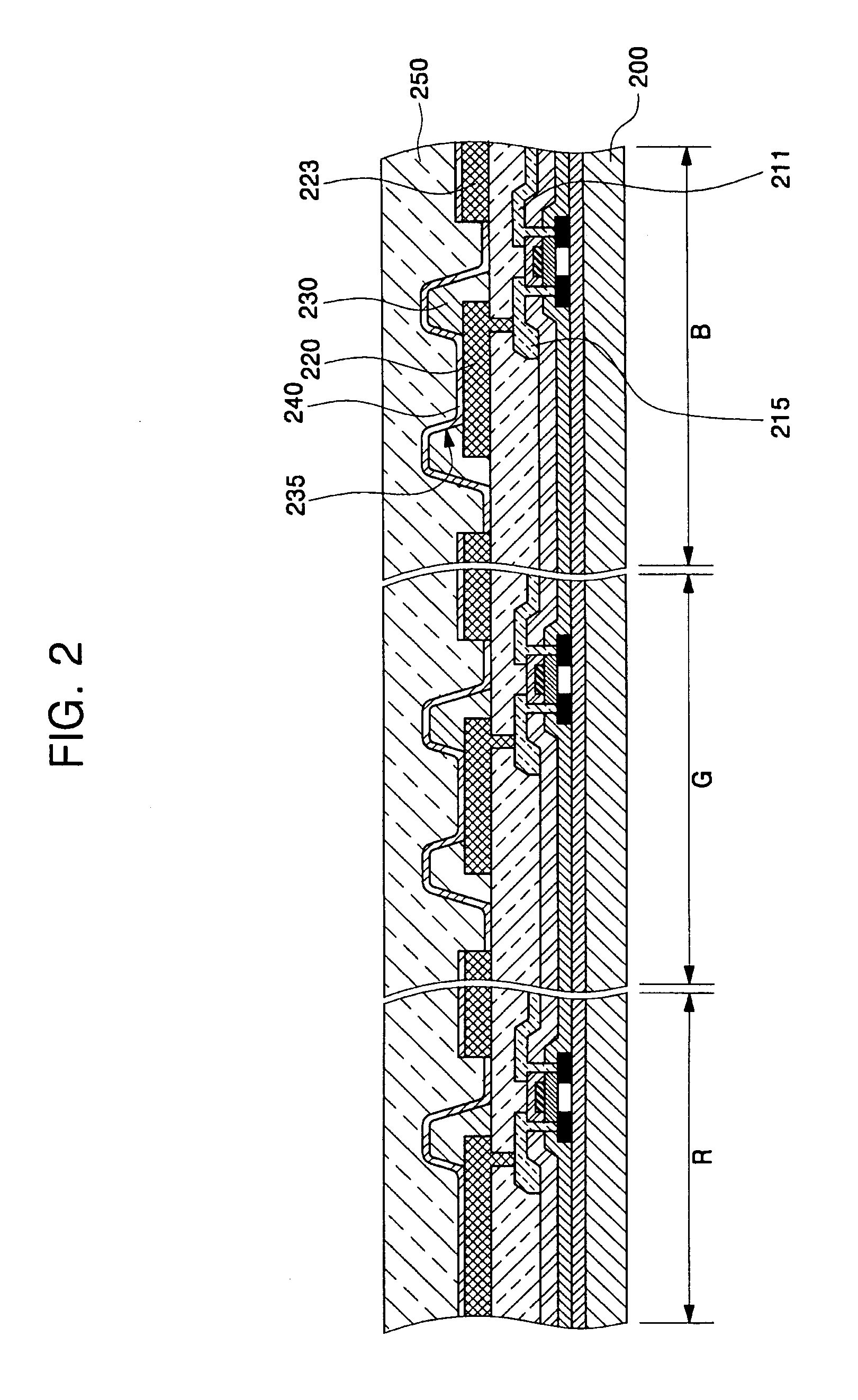
[0040]FIG. 2 is a partial cross-sectional view that illustrates a top emission organic light emitting diode (OLED) display according to a first exemplary embodiment of the present invention, partially showing R, G, and B unit pixels of the top emission OLED display.

[0041] Referring to FIG. 2, an active matrix organic light emitting diode (AMOLED) display accord...


PUM


Abstract

An organic light emitting diode (OLED) display. The OLED display includes: a lower electrode formed on a layer on an insulating substrate having a thin film transistor. The lower electrode is electrically connected to the thin film transistor. An auxiliary electrode is formed on the same layer as the lower electrode, and a pixel defining layer is formed on edges of the lower electrode, thereby defining an opening which exposes a portion of the lower electrode. An organic layer is formed on the portion of the lower electrode exposed by the opening, and an upper electrode is formed on an entire surface of the insulating substrate and electrically connected to the auxiliary electrode. An edge of the auxiliary electrode may have a taper angle of at least 90°.

Description

CROSS-REFERENCE TO RELATED APPLICATION [0001] This application claims priority to and the benefit of Korean Patent Application No. 10-2004-0023900, filed Apr. 7, 2004, and Korean Patent Application No. 10-2004-0024016, filed Apr. 8, 2004, the entire contents of both of which are incorporated herein by reference. BACKGROUND OF THE INVENTION [0002] 1. Field of the Invention [0003] The present invention relates to an organic light-emitting diode (OLED) display and a method of fabricating the same. More particularly, the present invention relates to a top emission OLED display using an auxiliary electrode for preventing or reducing a voltage drop of an upper electrode such that the top emission OLED display may be large-sized and a method of fabricating the same. [0004] 2. Description of the Related Art [0005] A conventional top emission active matrix organic light-emitting diode (AMOLED) display uses a transparent cathode electrode in order to emit light toward a sealing substrate. [00...

Claims


Application Information

Patent Timeline
IPC IPC(8): H01L27/15H01L27/32
CPCH01L27/3246H01L2227/323H01L51/5203H01L27/3276H10K59/122H10K59/131H10K59/1201H10K59/80522H10K50/824
Inventor LEE, KWAN-HEEKIM, EUN-AHSEO, CHANG-SUPARK, MOON-HEE
Owner SAMSUNG DISPLAY CO LTD
Features
  • Generate Ideas
  • Intellectual Property
  • Life Sciences
  • Materials
  • Tech Scout
  • Unparalleled Data Quality
  • Higher Quality Content
  • 60% Fewer Hallucinations
Learn More