Display element and display device

a display element and display device technology, applied in the field of display devices, can solve the problems of slow response, large hindrances to tn mode, narrow viewing angle, etc., and achieve the effects of easy temperature control, precise temperature control, and fast response speed

Active Publication Date: 2005-10-27
SHARP KK
View PDF10 Cites 41 Cited by
  • Summary
  • Abstract
  • Description
  • Claims
  • Application Information

AI Technical Summary

Benefits of technology

[0036] As described, because the conventional liquid crystal display element uses a change in an alignment direction of liquid crystal molecules, the response speed of the conventional liquid crystal display element is greatly influenced by intrinsic viscosity of liquid crystal. On the contrary, the aforementioned arrangement uses the change in the magnitude of the optical anisotropy in the medium so as to carry out displaying. For this reason, the response speed is not greatly influenced by the intrinsic viscosity of the liquid crystal unlike the conventional display element. Therefore, the arrangement allows realization of high-speed response. Further, the high-speed responsiveness of the present display element can be used for a field sequential color display device.
[0037] In the conventional display element, the driving temperature is limited to a vicinity of a Nematic phase / isotropic phase transition point, and therefore very precise temperature control is required. On the other hand, the present invention only requires maintenance of temperature at which the degree of optical anisotropy of the medium can be changed in response to application of an external field. Thus, the present invention allows easy temperature control.
[0038] With this arrangement, the medium exhibits optical isotropy when no electric field is applied, and becomes optically anisotropic when an electric field is applied. In this case, the shape of refractive index ellipsoid changes according to whether or not an electric field is applied. That is, the display is performed by not changing the direction of the optical anisotropy but changing the degree of optical anisotropy (orientational order, refractive index). Therefore, it is possible to realize a display element with a wider range of driving temperature, a wider viewing angle characteristic, and high-speed response, in contrast to the conventional display element performing display by changing the direction of the optical anisotropy. Further, the display element of the present invention may be arranged so that the medium exhibits optical anisotropy when no electric field is applied, and becomes optically isotropic when an electric field is applied. This arrangement also ensures effects of a wider viewing angle characteristic, and high-speed response.
[0039] Further, the horizontal / vertical alignment film ensures the alignment of medium even when the display element is turned on at a temperature lower than the phase transition temperature where the medium is not heated up enough for driving, that is, it has different physical condition to that for allowing-driving. Therefore, the optical contribution of the medium (with a different physical condition to that under the driving is possible) can be cancelled. On this account, it is possible to realize superior display before the display element is heated up. However, if the alignment film is formed above the electric field applying means, the effective voltage application to the medium, that is effective voltage application to the display medium is reduced.
[0040] In this view, with the foregoing arrangement, the electric field applying means, which generates an electric field in a direction parallel to the substrates so as to apply the electric field to the medium to cause optical modulation of the medium, is provided on one (a first substrate) of the pair of substrates; and a horizontal or vertical alignment film is provided on the other (second substrate) of the pair of substrates. In this arrangement, the horizontal / vertical alignment film is not provided on the substrate where the electric field applying means is provided. In this arrangement, the application of electric field from the electric field applying means to the medium is not performed through the alignment film. Therefore, the voltage level is not decreased because of the alignment film, and the driving voltage of the display element does not need to be increased, thereby ensuring reduction of driving voltage.
[0042] Therefore, according to the present invention, it is possible to obtain a display device with a wider driving temperature range, high-speed response, and superior viewing angle.

Problems solved by technology

However, the TN mode liquid crystal display element has some drawbacks such as slow response, a narrow viewing angle etc.
Those disadvantages are large hindrances for the TN mode to take over CRT (Cathode Ray Tube).
The mode using the FLC or AFLC allows high-speed response and wide viewing angle, but is inadequate in terms of shock resistance or temperature characteristics.
Such a defect has kept the FLC or AFLC display device from wide and practical application.
However, the polymer dispersed liquid crystal display mode has a problem in its response property upon image display.
Further, each of the display modes uses rotation of the liquid crystal molecules caused by electric field application, wherein the liquid crystal molecules rotate together maintaining the alignment, thus a response speed is slow.
In the meantime, the mode using the FLC or AFLC is superior in response speed and viewing angle, but the mode has a problem of irreversible alignment breakdown due to external force.
However, those conventional display elements have not achieved significant reduction of driving voltage; and therefore are not sufficient for practical use.

Method used


Image

  • Display element and display device
  • Display element and display device
  • Display element and display device

Examples


second embodiment

[0259] The following will explain another embodiment of the present invention with reference to FIG. 7. The following embodiment basically explains only the difference from First Embodiment. For ease of explanation, materials having the equivalent functions as those shown in the drawings pertaining to First Embodiment above will be given the same reference symbols, and explanation thereof will be omitted here.

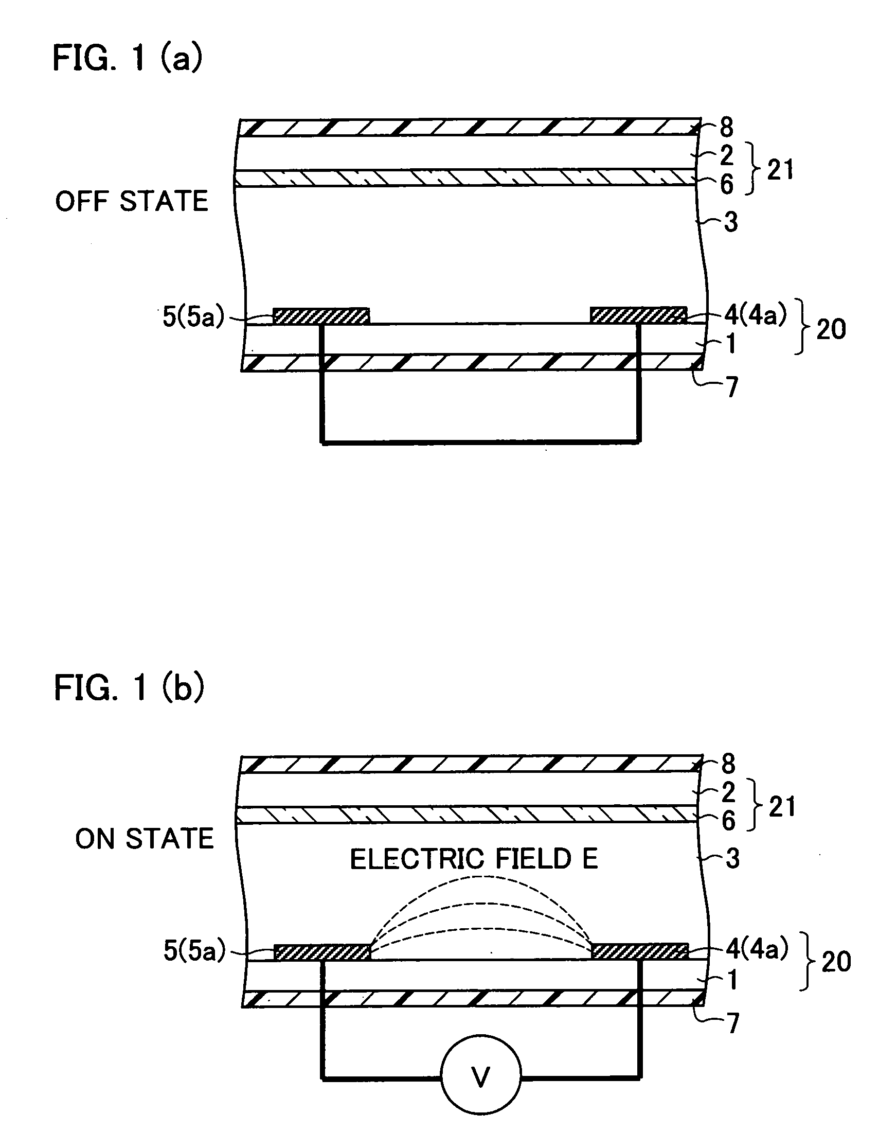
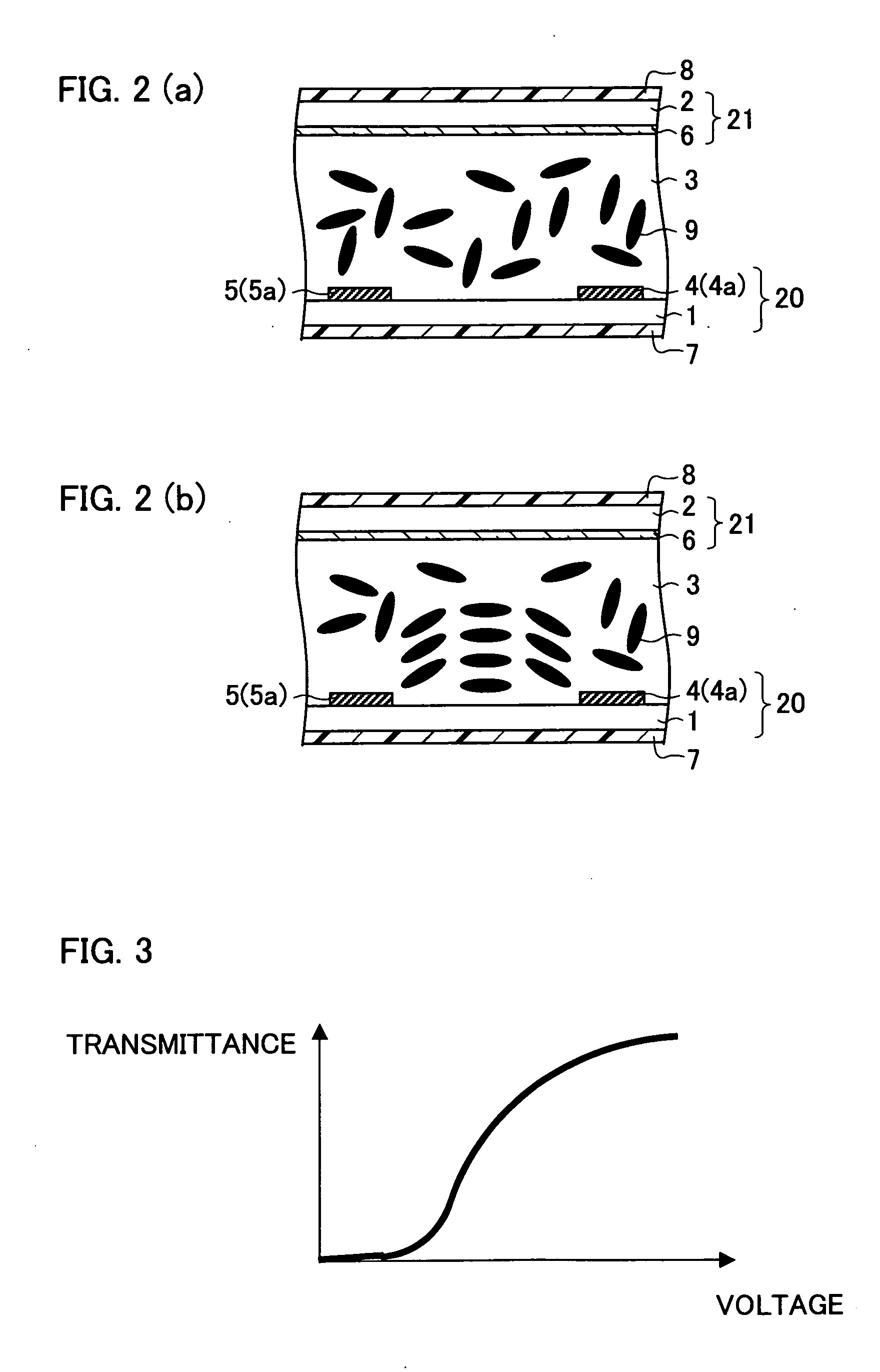
[0260] As with First Embodiment above, in the display element according to the present embodiment, there is no alignment film on the substrate 1 where the electrodes 24 and 25 are formed. Therefore, in the display element of the present embodiment, voltage application from the electrodes 24 and 25 to the medium A in the medium layer 3 is not performed via the alignment film. Therefore, in the display element of the present embodiment, the voltage amount applied to the medium A does not decrease, thereby achieving significant reduction in driving voltage.

[0261] In First Embodi...


PUM

PropertyMeasurementUnit
angleaaaaaaaaaa
angleaaaaaaaaaa
selective wavelength rangeaaaaaaaaaa

Abstract

The subject invention provides a display element which achieves reduction in driving voltage. The display element according to the present invention includes substrates 1 and 2, at least one of which is transparent, and a medium layer 3 held between the substrates 1 and 2, the display element further including on the substrate 1 electrodes 4 and 5 for generating an electric field in a direction substantially parallel to the substrates so as to apply the electric field to the medium layer3 to cause optical modulation of the medium; and an alignment film 6 which is provided on the surface of the substrate 2. With this arrangement, the voltage level is not decreased because of the alignment film 6, and the driving voltage of the display element does not need to be increased, thereby ensuring reduction of driving voltage.

Description

[0001] This Nonprovisional application claims priority under 35 U.S.C. § 119(a) on Patent Application No. 2004 / 131972 filed in Japan on Apr. 27, 2004, and No. 2005 / 121713 filed in Japan on Apr. 19, 2005, the entire contents of which are hereby incorporated by reference. FIELD OF THE INVENTION [0002] The present invention relates to a display device, particular to a display element and a display device with high-speed response and wide viewing angle. BACKGROUND OF THE INVENTION [0003] A liquid crystal display element has advantages over other display element in terms of thinness, lightness in weight, and low power consumption. With these advantages, the liquid crystal display element is widely used for image display devices such as a television or a video, a monitor, OA (Office Automation) equipments such as a word processor, and a personal computer. [0004] There are conventionally well-known liquid crystal display modes for the liquid crystal display element, such as the TN (Twisted...

Claims


Application Information

Patent Timeline
Patent Type & Authority Applications(United States)
IPC IPC(8): G02F1/1334C09K19/02G02F1/1335G02F1/1337G02F1/1343G02F1/139
CPCC09K19/02G02F1/1392G02F1/134363
Inventor SHIBAHARA, SEIJIINOUE, IICHIROMIYACHI, KOICHI
Owner SHARP KK
Why Eureka
Try Eureka