Antenna line protection device

a line protection and antenna technology, applied in the direction of electrical equipment, earthing switch association, coupling protection earth/shielding arrangement, etc., can solve the problems of high-power emp influence, semiconductor parts used in radar systems are very sensitive, and semiconductor parts are vulnerable to the influence of high-power emps

Active Publication Date: 2015-11-17
ELECTRONICS & TELECOMM RES INST
View PDF10 Cites 0 Cited by
  • Summary
  • Abstract
  • Description
  • Claims
  • Application Information

AI Technical Summary

Benefits of technology

[0011]At least one embodiment of the present invention is intended to provide an antenna line protection device that includes a streamer discharge module coupled between a pair of coaxial connectors and configured to suppress an excessive input pulse, thereby achieving a discharge tube response speed equal to or shorter than a nanosecond.
[0012]At least one embodiment of the present invention is intended to provide an antenna line protection device in which a cone-shaped impedance matching unit is disposed inside the coaxial connector between the inner circumferential surface of a through hole and the outer circumferential surface of a first center electrode, thereby overcoming impedance mismatch between a commercial N-connector using a dielectric, such as a Teflon, and a coaxial line using air as a dielectric.
[0014]In accordance with an aspect of the present invention, there is provided an antenna line protection device, including a pair of coaxial connectors disposed on both side ends of the antenna line protection device; and a streamer discharge module coupled between the coaxial connectors so that, when a pulse signal is input via the coaxial connectors, the streamer discharge module induces an electric field and thus establishes a discharge current channel, thereby suppressing an excessive input pulse.

Problems solved by technology

In general, semiconductor parts used in radar systems are very sensitive.
Accordingly, such semiconductor parts may be easily damaged by, in particular, electromagnetic waves.
Such semiconductor parts are vulnerable to the influence of a high-power EMP, a high-power microwave (HAM) pulse and an ultra wide band (UWB) pulse.
Accordingly, military and civil communication systems including electronic equipment unprotected from the above-described pulses may be rendered useless due to equipment that generates such pulses.

Method used


Image

  • Antenna line protection device
  • Antenna line protection device
  • Antenna line protection device

Examples


Embodiment Construction

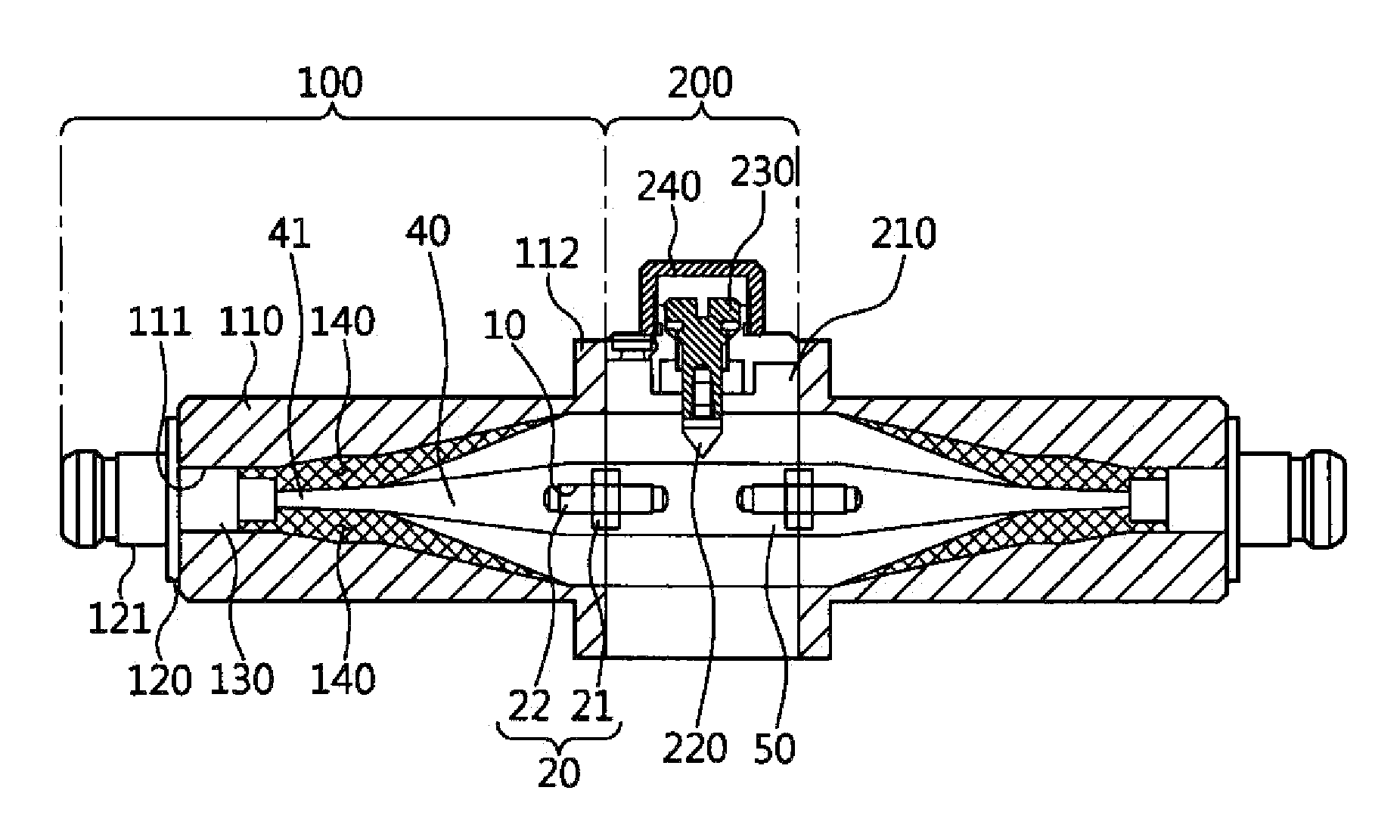
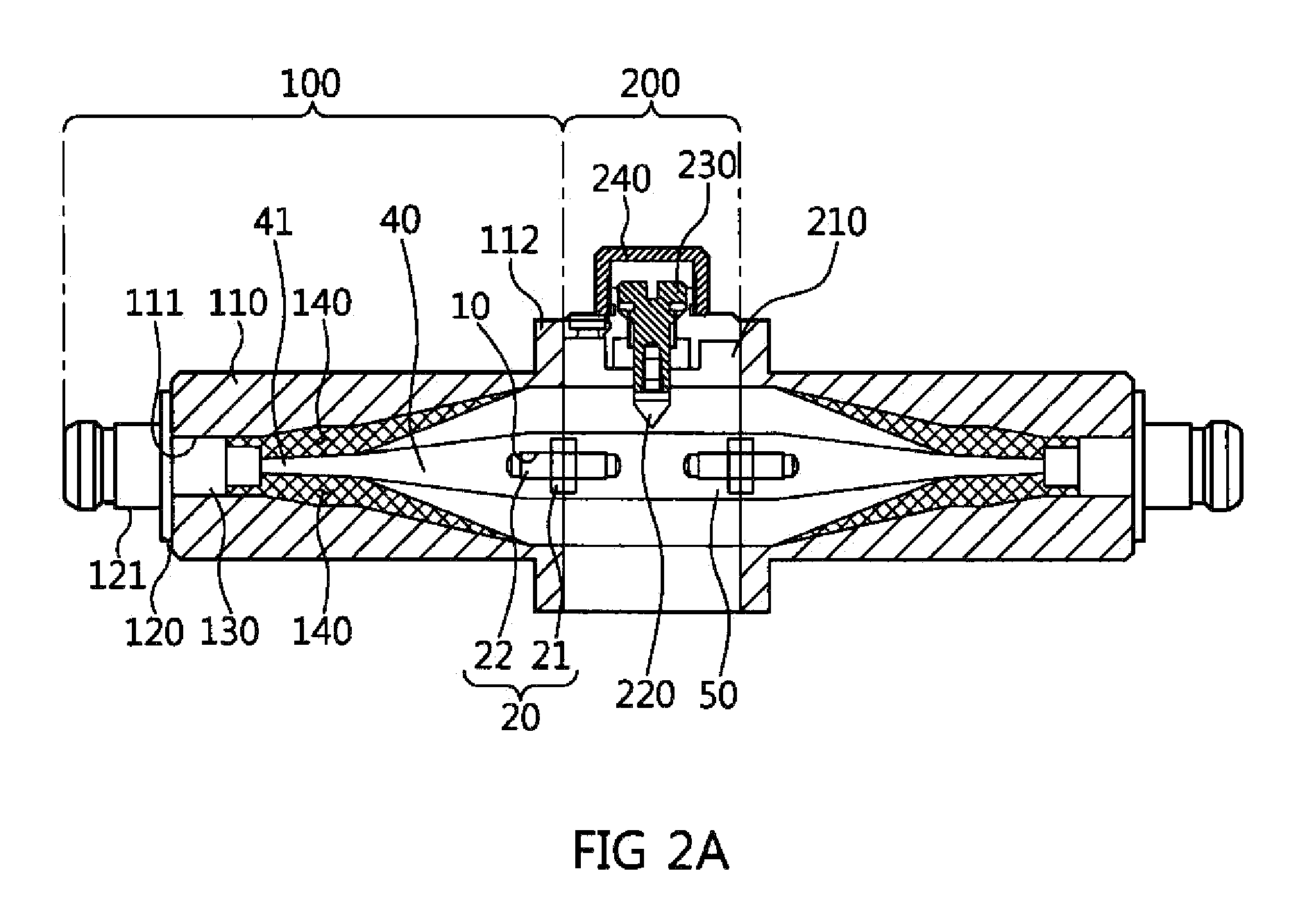
[0043]Embodiments of the present invention are described in detail below with reference to the accompanying drawings. Repeated descriptions and descriptions of known functions and configurations which have been deemed to make the gist of the present invention unnecessarily obscure will be omitted below. The embodiments of the present invention are intended to fully describe the present invention to a person having ordinary knowledge in the art to which the present invention pertains. Accordingly, the shapes, sizes, etc. of components in the drawings may be exaggerated to make the description clear.

[0044]The present invention is directed to an antenna line protection device for protecting the antenna line of a wireless communication system from high-power electromagnetic pulses or intentional electromagnetic wave interference signals.

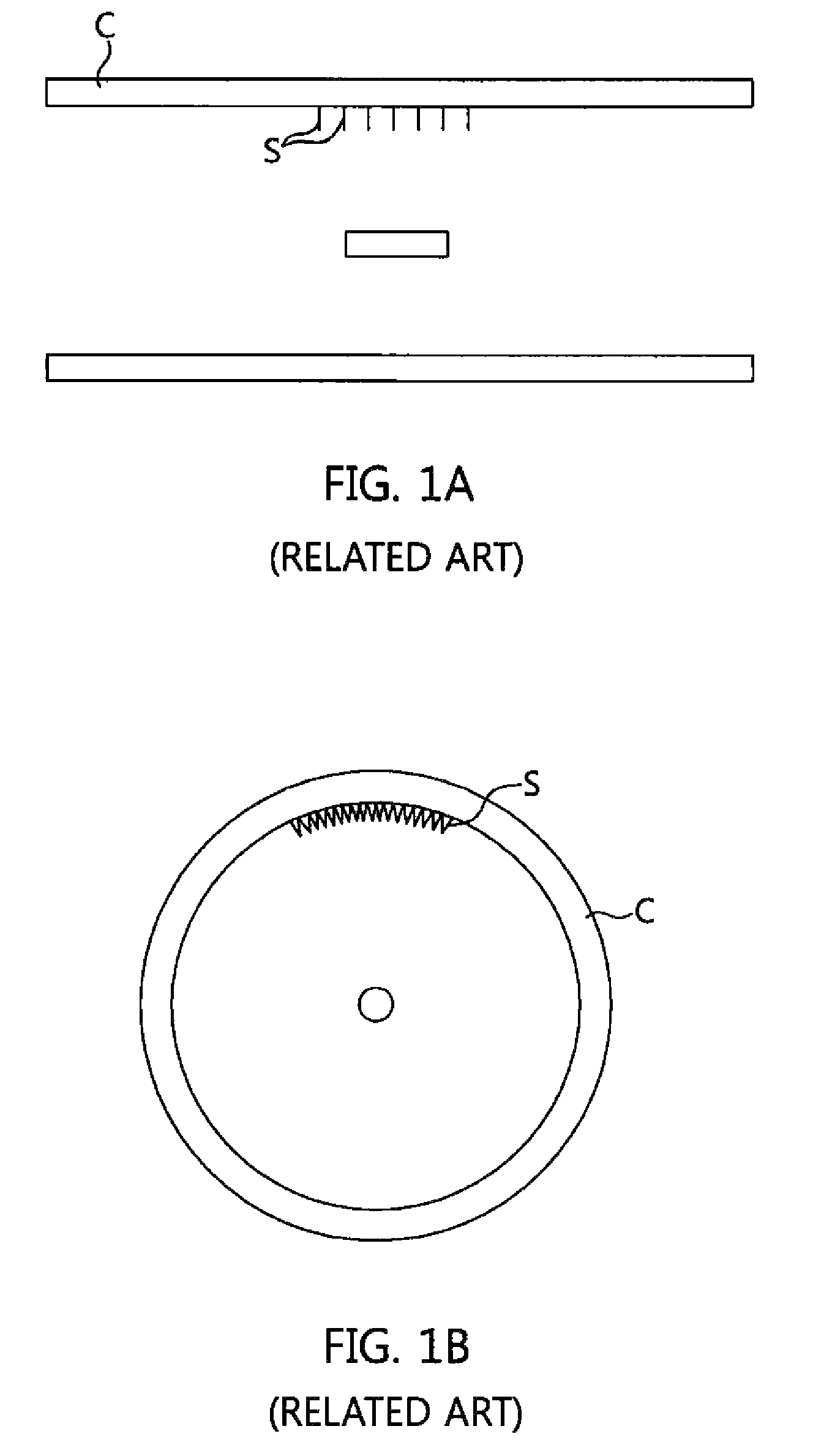
[0045]For this purpose, a gas discharge tube has been used so far. However, the gas discharge tube cannot eliminate a high-power electromagnetic pulse h...


PUM


Abstract

An antenna line protection device includes a pair of coaxial connectors and a streamer discharge module. The pair of coaxial connectors are disposed on both side ends of the antenna line protection device. The streamer discharge module is coupled between the coaxial connectors so that, when a pulse signal is input via the coaxial connectors, the streamer discharge module induces an electric field and thus establishes a discharge current channel, thereby suppressing an excessive input pulse.

Description

CROSS REFERENCE TO RELATED APPLICATIONS[0001]This application claims the benefit of Korean Patent Application Nos. 10-2013-0079191 and 10-2013-0124714, filed on Jul. 5, 2013 and Oct. 18, 2013, respectively, which are hereby incorporated by reference herein in their entirety.BACKGROUND OF THE INVENTION[0002]1. Technical Field[0003]The present disclosure relates to an antenna line protection device for protecting the electronic elements and devices of an antenna line from high-power electromagnetic wave pulses and, more particularly, to an antenna line protection device that is capable of providing high-power signal limiting performance at a response speed equal to or shorter than a nanosecond using a streamer discharge principle in order to protect the electronic parts of the antenna line of a wireless communication system from a high-power electromagnetic pulse (EMP) or an intentional electromagnetic interference (IEMI) signal.[0004]2. Description of the Related Art[0005]In general,...

Claims


Application Information

Patent Timeline
Patent Type & Authority Patents(United States)
IPC IPC(8): H01R13/648H01Q1/50H01P1/30H01P5/02
CPCH01Q1/50H01P1/30H01P5/026
Inventor RYU, SEUNG-KABLEE, KYUNG-HOONCHU, KWANG-UKKIM, UIJUNGNAMKOONG, UP
Owner ELECTRONICS & TELECOMM RES INST
Why Eureka
Try Eureka