Display, wiring board, and method of manufacturing the same

a technology of wiring board and display panel, which is applied in the direction of optics, electrical apparatus construction details, instruments, etc., can solve the problems of long exposure step, complex exposure step, and difficulty in executing full plate exposure for the entire display region and peripheral region, so as to shorten the time necessary for the exposure step, the effect of reducing the number of mask patterns

Active Publication Date: 2005-11-03
JAPAN DISPLAY CENTRAL CO LTD
View PDF6 Cites 19 Cited by
  • Summary
  • Abstract
  • Description
  • Claims
  • Application Information

AI Technical Summary

Benefits of technology

[0013] It is an object of the present invention to minimize the number of mask patterns to be used in a photolithography process in manufacturing a display or a wiring board used for it, thereby shortening the time necessary for the exposure step.
[0014] It is another object of the present invention to reduce the variation in wiring pattern shape caused by the manufacturing process, and in the field of displays, realize a higher display quality.

Problems solved by technology

For this reason, in manufacturing a display, it is difficult to execute full plate exposure for the entire display region and peripheral region.
As described above, in the display manufacturing process, a complex exposure step is necessary, and the exposure step requires long time.
As a result, since the number of times of exposure (the number of shots) increases, the time required for the exposure step cannot be shortened.

Method used


Image

  • Display, wiring board, and method of manufacturing the same
  • Display, wiring board, and method of manufacturing the same
  • Display, wiring board, and method of manufacturing the same

Examples


first embodiment

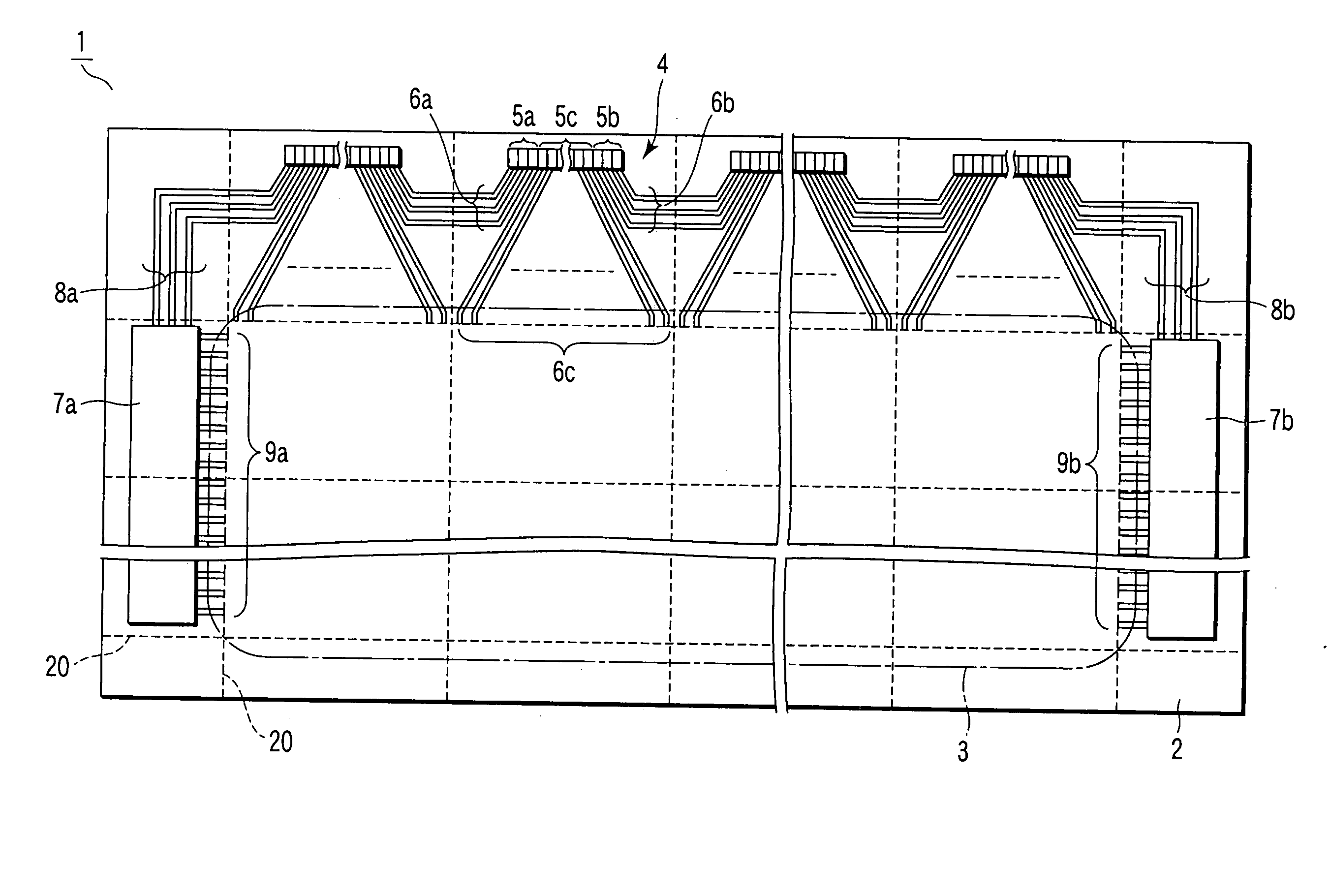
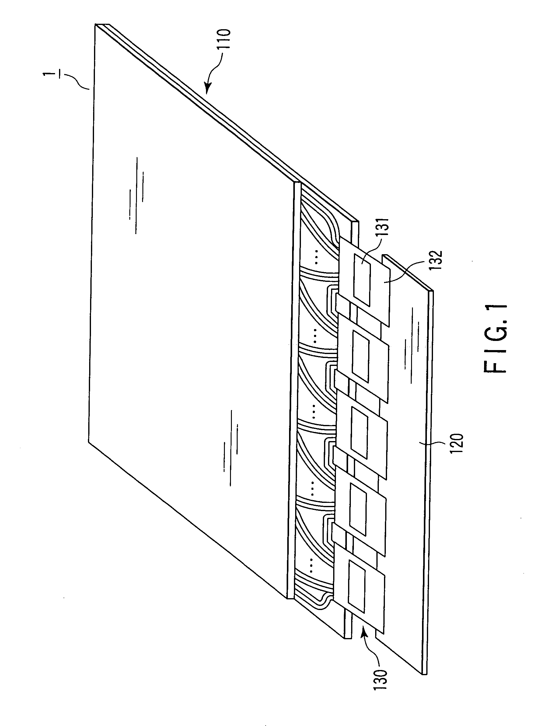
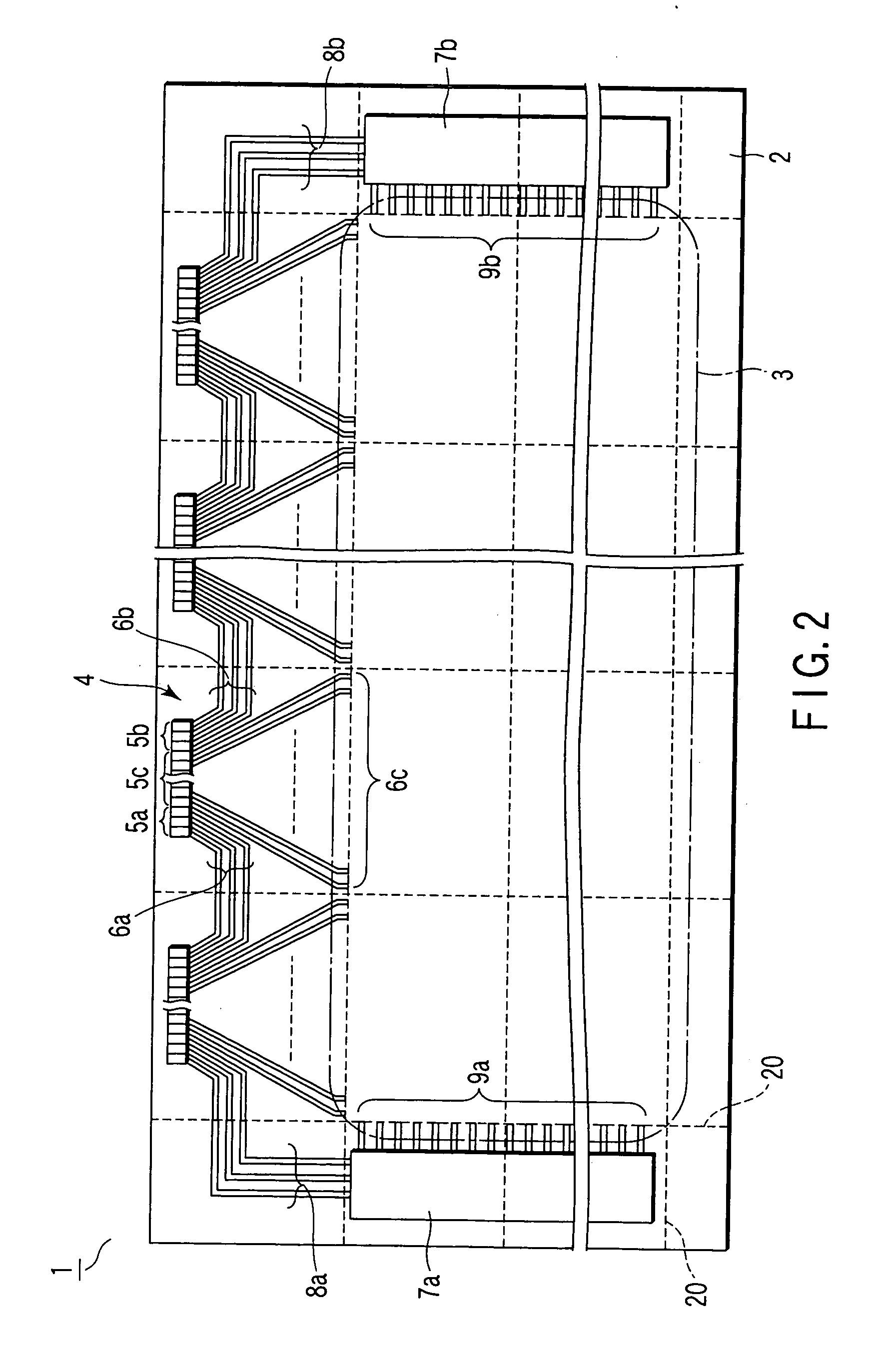
[0032]FIG. 1 is a perspective view schematically showing a display according to the present invention. FIG. 2 is a plan view schematically showing part of the display shown in FIG. 1. A display 1 is, e.g., an organic EL display or liquid crystal display. The display includes a display panel 110, a driving circuit board 120 on which circuits (not shown) which drive the display panel 110 are mounted, and a connection means 130 for electrically connecting the display panel 110 to the driving circuit board 120. In this embodiment, the connection means 130 is a TCP (Tape Carrier Package) formed by mounting driving ICs 131 on flexible substrates 132.

[0033] The display panel 110 includes an insulating substrate 2 made of, e.g., glass. A display region 3 and a peripheral region outside it are defined on one major surface of the substrate 2.

[0034] A plurality of pixels (not shown) are arrayed in a matrix on the display region 3. Each pixel includes a pixel circuit and a display element.

[00...

second embodiment

[0063] The second embodiment will be described next.

[0064]FIG. 9 is a plan view schematically showing part of a display according to the second embodiment of the present invention. The display according to this embodiment has almost the same structure as that of the display according to the first embodiment except the following point. In this embodiment, as shown in FIG. 9, a display panel 110 has a terminal 15 and a wiring line 16. The wiring line 16 surrounds the display region. The terminal 15 is arranged along the wiring line 16 and a wiring line included in wiring line groups 6a and 6b which is farthest from the display region. When the terminal 15 is used, any of the wiring lines included in the wiring line groups 6a and 6b can be used. The wiring line is not limited to that farthest from the display region.

[0065] When this structure is employed, and the display panel 110 is a liquid crystal display panel, the terminal 15 and wiring line 16 can be used as a transfer pad and a...

third embodiment

[0068] The third embodiment will be described next.

[0069]FIG. 10 is a plan view schematically showing part of a display according to the third embodiment of the present invention. The display according to this embodiment has almost the same structure as that of the display according to the second embodiment except the following point. In this embodiment, as shown in FIG. 10, part of a video signal line driver and, in this example, distribution circuits 17 are arranged in the peripheral region of a display panel 110. The distribution circuit 17 supplies a video signal to video signal lines through a wiring line group 6d in accordance with a signal supplied through a wiring line group 6c and a wiring line 18. In this way, various modifications or additions can be done for a connection portion 4.

[0070] In the first to third embodiments, the display region 3 is segmented, as shown in FIGS. 2, 9, and 10, and exposure of the photoresist film is executed seuentialy for each segmented part...


PUM

PropertyMeasurementUnit
shapeaaaaaaaaaa
conductiveaaaaaaaaaa
insulatingaaaaaaaaaa

Abstract

Provided is a wiring board including an insulating substrate with a first region and a second region adjacent to each other on a major surface, signal line groups arrayed on the first region, and connection portions arranged on the second region in correspondence with the signal line groups, wherein each connection portion includes first to third terminal groups, a first wiring line group connecting the first terminal group to the corresponding signal line group, a second wiring line group connected to the second terminal group, and a third wiring group connected to the third terminal group, wherein the second and third wiring line groups are connected to each other between each adjacent connection portions, and all of the connection portions are the same in shapes of the first to third terminal groups and the first to third wiring line groups.

Description

CROSS REFERENCE TO RELATED APPLICATIONS [0001] This is a Continuation Application of PCT Application No. PCT / JP2004 / 000814, filed Jan. 29, 2004, which was published under PCT Article 21(2) in Japanese. [0002] This application is based upon and claims the benefit of priority from prior Japanese Patent Application No. 2003-022507, filed Jan. 30, 2003, the entire contents of which are incorporated herein by reference.BACKGROUND OF THE INVENTION [0003] 1. Field of the Invention [0004] The present invention relates to a display, wiring board, and method of manufacturing the same. [0005] 2. Description of the Related Art [0006] In a display such as a liquid crystal display or organic EL (Electroluminescent) display, wiring line groups of flexible tapes are connected to OLB (Outer Lead Bonding) pad groups formed on a display panel to make it possible to supply a power or signal from the outside of the display panel to circuits in the panel. For example, in a display on which a control driv...

Claims


Application Information

Patent Timeline
Patent Type & Authority Applications(United States)
IPC IPC(8): G02F1/1345
CPCG02F1/1345
Inventor AOKI, YOSHIRO
Owner JAPAN DISPLAY CENTRAL CO LTD
Why Eureka
Try Eureka