Method for fractionating single-wall carbon nanotubes

a carbon nanotube and single-wall technology, applied in the field of macroscopy manipulable nanoscale devices, can solve the problems of affecting the development of mechanical, electrical, chemical and biological devices and systems that include or comprise nanoscale components, sometimes termed nanotechnology, and the inability to meet the requirements of nanoscale components, etc., to achieve accurate data interpretation, easy to make electrically conductive, and easy to damage

Inactive Publication Date: 2005-11-03
RICE UNIV
View PDF20 Cites 38 Cited by
  • Summary
  • Abstract
  • Description
  • Claims
  • Application Information

AI Technical Summary

Benefits of technology

[0011] The nanoscale devices according to the present invention provide strong, reliably mounted probe tips and other nanoscale fabricators and manipulators, that are gentle, hard to damage, even upon “crashing” into the working surface, that can be easily made electrically conductive, that can present a uniform diameter and precisely known atomic configuration, including precisely located derivitization with chemical moieties.
[0012] The devices of the present invention have a number of advantages over conventional microscopy probes (e.g. STM and AFM). A probe tip consisting of a single molecular nanotube or a few such tubes has the advantage that all its constituent atoms are covalently bonded in place and are unlikely to move, even under extreme stress, such as that occurring when the tip “crashes” into the object being imaged. Moreover, the known, stable geometry of molecular nanotube tips allows one to more accurately interpret the data acquired by probe microscopes using such tips. In addition, molecular nanotubes are very compliant, buckling in a gentle, predictable, and controllable fashion under forces that are small enough to avoid substantial deformation to delicate sample objects. Unlike currently used pyramidal probe tips, molecular nanotubes are very long with respect to their diameter, and can therefore reliably image the bottom areas of holes and trenches in the items being imaged.
[0013] Electrically conducting nanotube tips can be coated with an insulating material to achieve localized electrical activity at the end of the probe element. This geometry facilitates probing of electrochemical and biological environments.

Problems solved by technology

The development of mechanical, electrical, chemical and biological devices and systems that include or comprise nanoscale components, sometimes termed nanotechnology, has been slowed by the unavailability of or limitations inherent in devices that enable sensing, measuring, analyzing, and modifying objects with nanometer resolution and sensing, measuring, analyzing, moving, manipulating, fabricating and modifying objects with nanometer dimensions.
While good progress has been made in controlling the position of the macroscopic probe to sub-angstrom accuracy and in designing sensitive detection schemes, the tip designs to date have a number of problems.
One such problem arises from changes in the properties of the tip as atoms move about on the tip, or as the tip acquires an atom or molecule from the object being imaged.
Another difficulty with existing probe microscope tips is that they typically are pyramidal in shape, and that they are not able to penetrate into small “holes” on the object being imaged, and they may give false image information around sharp vertical discontinuities (e.g., steps) in the object being imaged, because the active portion of the “tip” may shift from the bottom atom to an atom on the tip's side.
Moreover, conducting conventional probe microscope tips have never been successfully covered with an insulating material so that the only electrically-active element is the point of the tip itself.

Method used


Image

  • Method for fractionating single-wall carbon nanotubes
  • Method for fractionating single-wall carbon nanotubes
  • Method for fractionating single-wall carbon nanotubes

Examples


Embodiment Construction

[0032] The preferred embodiment of the present invention and its advantages are best understood by referring to FIGS. 1 through 13 of the drawings, like numerals being used for like and corresponding parts of the various drawings.

Macroscopically Manipulable Nanoscale Devices

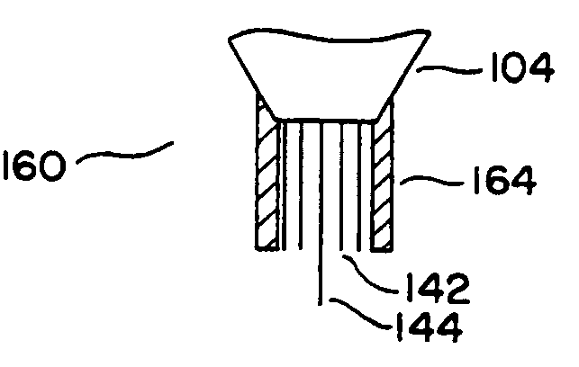
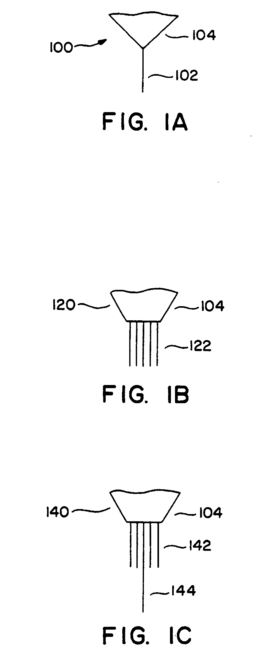
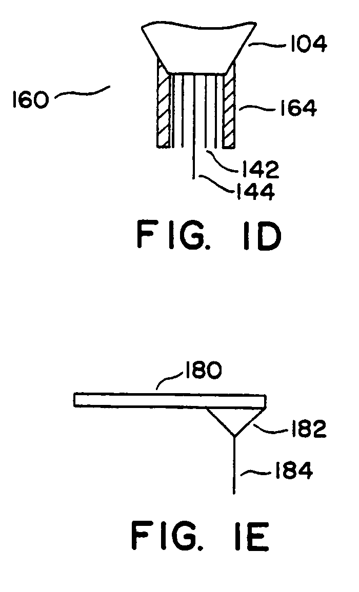
[0033] Broadly, the macroscopically manipulable nanoscale devices of the present invention comprise a nanotube assembly attached to a mounting element that permits macroscopic manipulation or observation. In a preferred form this device comprises a nanotube probe tip assembly made up of one or more single-wall and / or multi-wall nanotubes. This assembly is connected to a mounting element at one end, with the other end being free and capable of coming into direct contact or near proximity to the object being sensed, measured, analyzed, moved, manipulated, and / or modified. The free “sensing end” has a transverse dimension in the nanometer range. The “sensing end” interacts with objects being sensed, measured, ana...


PUM

PropertyMeasurementUnit
diametersaaaaaaaaaa
diametersaaaaaaaaaa
diametersaaaaaaaaaa

Abstract

The invention relates generally to dispersing and fractionating single-wall carbon nanotubes, which can be derivatized to facilitate fractionation, for example, by adding solubilizing moieties to the nanotubes.

Description

TECHNICAL FIELD OF THE INVENTION [0001] This invention relates generally to the field of macroscopically manipulable nanoscale devices that permit information to be provided to or obtained form a nanoscale environment, and more particularly to the use of nanotubes attached to macroscale mounting members as nanoscale probes, fabricators and manipulators. BACKGROUND OF THE INVENTION [0002] The development of mechanical, electrical, chemical and biological devices and systems that include or comprise nanoscale components, sometimes termed nanotechnology, has been slowed by the unavailability of or limitations inherent in devices that enable sensing, measuring, analyzing, and modifying objects with nanometer resolution and sensing, measuring, analyzing, moving, manipulating, fabricating and modifying objects with nanometer dimensions. [0003] One class of devices that have found some use in nanotechnology applications are proximity probes of various types including those used in scanning...

Claims


Application Information

Patent Timeline
Patent Type & Authority Applications(United States)
IPC IPC(8): G01B7/34B82B1/00B82B3/00C01B31/02D01F9/12D01F9/127G01B21/30G01N33/543G01Q70/12G11B9/00G11B11/00G21K7/00
CPCB82Y10/00Y10T428/2918B82Y30/00B82Y35/00B82Y40/00C01B31/0213C01B31/0233C01B31/0273C01B2202/02C01B2202/06C01B2202/08C01B2202/24C01B2202/34G01Q70/12G01Q70/16G11B9/1409G11B11/007G11C13/025G11C2213/81H01J2201/30469Y10S977/70Y10S977/75Y10S977/843Y10S977/845Y10S977/789B82Y15/00C01B32/154C01B32/162C01B32/174Y10T428/249977
Inventor COLBERT, DANIEL T.DAI, HONGJIEHAFNER, JASON H.RINZLER, ANDREW G.SMALLEY, RICHARD E.LIU, JIESMITH, KENNETH A.GUO, TINGNIKOLAEV, PAVELTHESS, ANDREAS
Owner RICE UNIV
Why Eureka
Try Eureka