Method for integrating image sensor

Active Publication Date: 2005-11-03
INTELLECTUAL VENTURES II
View PDF5 Cites 23 Cited by
  • Summary
  • Abstract
  • Description
  • Claims
  • Application Information

AI Technical Summary

Benefits of technology

[0011] It is, therefore, an object of the present invention to provide a method for integrating an image sensor c

Problems solved by technology

Meanwhile, if a light source is different, a flicker noise appears.
However, in case of using t

Method used


Image

  • Method for integrating image sensor
  • Method for integrating image sensor
  • Method for integrating image sensor

Examples


Embodiment Construction

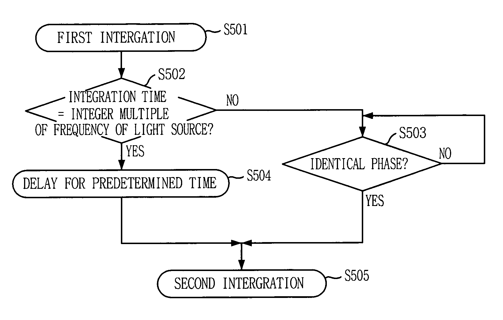
[0020] Hereinafter, detailed descriptions on preferred embodiments of the present invention will be provided with reference to the accompanying drawings.

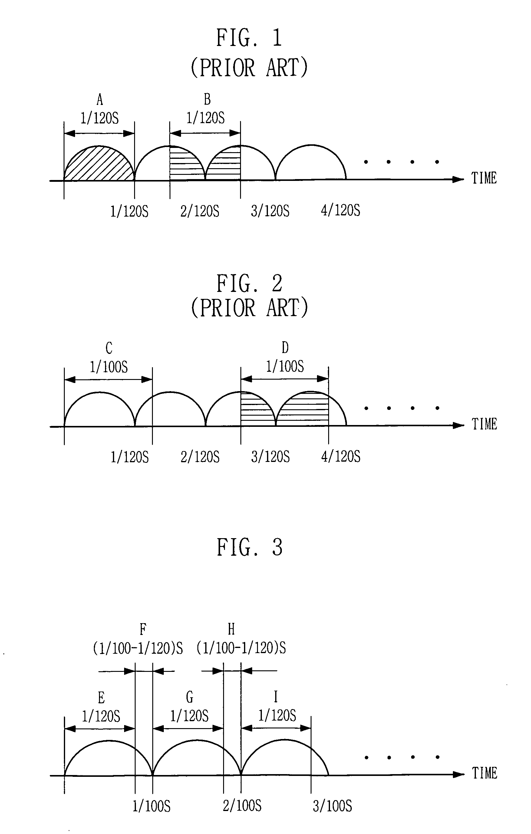
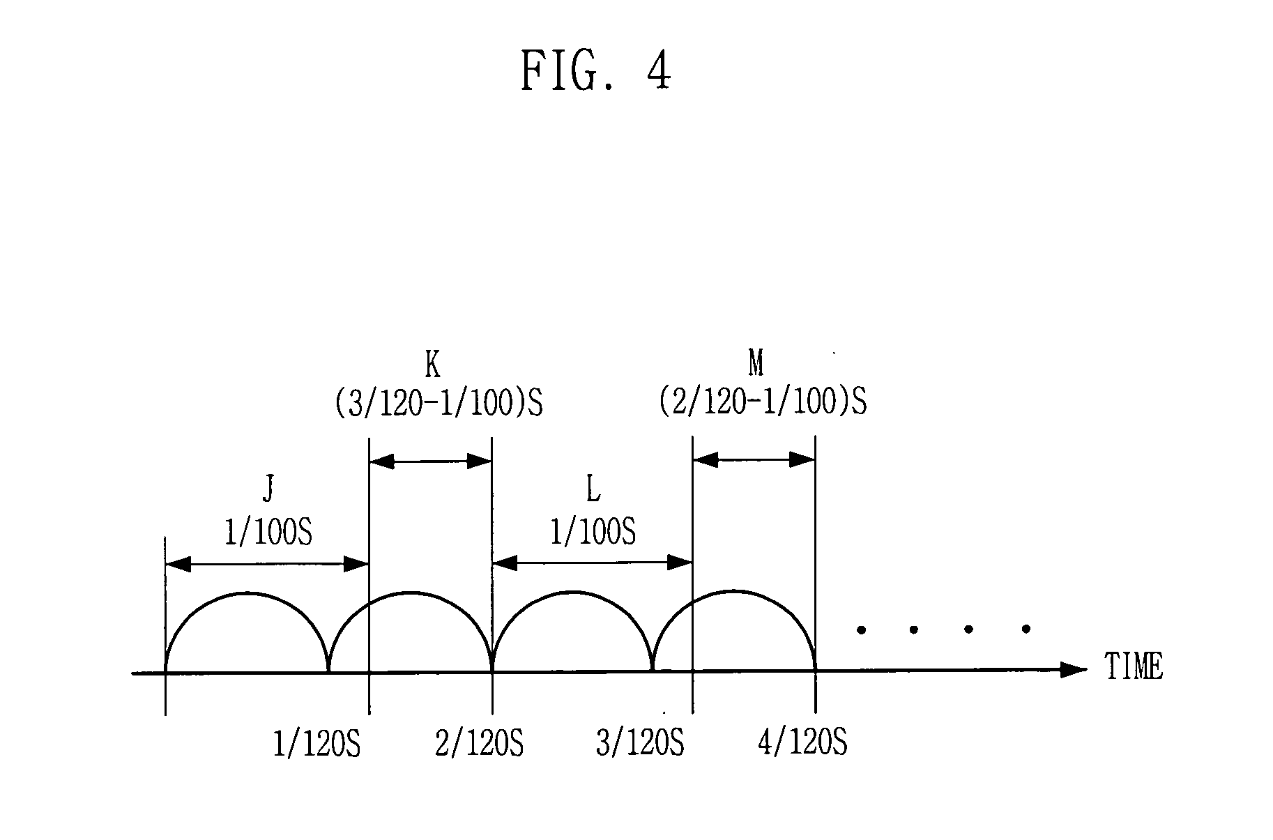
[0021] A flicker noise phenomenon happens because a frequency of a light source and an integration time of an image sensor are different from each other. A light source is a light generator used in our daily life. Accordingly, the sun is an example of the light source and a fluorescent lamp is also an example of the light source. In case of the sun light, the frequency is fairly high and thus, the integration time is always several thousands times greater than a sun light period. Therefore, the flicker noise is not generated under the sun light.

[0022] However, in case of the fluorescent lamp, the frequency is approximately 50 Hz or approximately 60 Hz, thereby causing the flicker noise as to an image sensor having an integration time of several tens ms.

[0023] A reason why various methods are applied to a CMOS image sensor to remo...


PUM


Abstract

Disclosed is a method for integrating an image sensor capable of removing a flicker noise without causing any burdens on a hardware due to setting up additional logics. The method for integrating an exposure time of an image sensor employing a line scan method, including the steps of: performing an integration to a first line when an integer multiple of a light source frequency is different from an integration time; and performing an integration to a second line at a phase substantially equal to a phase in which the integration to the first line is started.

Description

FIELD OF THE INVENTION [0001] The present invention relates to an image sensor; and more particularly, to a method for integrating an image sensor capable of removing a flicker noise. DESCRIPTION OF RELATED ARTS [0002] An image sensor is a device generating an image by using a characteristic that a semiconductor device reacts to a light. That is, the image sensor is a device that reads an electric value by sensing a brightness and a wavelength of each different light coming from a subject. The image sensor serves a role in changing the electric value into a level capable of a signal process. [0003] That is, an image sensor is a semiconductor device that converts an optical image into electrical signals. In the image sensors, a charge coupled device (CCD) is the semiconductor device that each of metal-oxide-silicon (MOS) capacitors are placed in close proximity and charge carriers are stored in or transferred between capacitors. CMOS image sensors are devices adopting a switching met...

Claims


Application Information

Patent Timeline
IPC IPC(8): H01L27/146H04N5/21H03F1/26H04N5/235
CPCH01L27/14601H04N5/2357H04N5/2353H04N23/73H04N23/745H04N5/21
Inventor HAN, HYUNG-JUNLIM, MOO-SUP
Owner INTELLECTUAL VENTURES II
Why Eureka
Try Eureka