Simplified wafer alignment

a technology of simplified wafers and wafers, applied in the direction of semiconductor/solid-state device testing/measurement, semiconductor/solid-state device details, instruments, etc., can solve the problems of adversely affecting the implantation process and resulting semiconductor devices, difficult to capture wafers via vacuum, and unfavorable degree of channeling, so as to mitigate particle contamination and mitigate particle contamination.

Active Publication Date: 2005-11-10
AXCELIS TECHNOLOGIES
View PDF15 Cites 13 Cited by
  • Summary
  • Abstract
  • Description
  • Claims
  • Application Information

AI Technical Summary

Benefits of technology

[0011] The present invention is directed to aligning wafers within semiconductor fabrication tools. More particularly, one or more aspects of the present invention pertain to quickly and efficiently finding an alignment marking, such as an alignment notch, on a wafer to allow the wafer to be appropriately oriented within an alignment tool. Unlike conventional systems, the notch is located without firmly holding and spinning or rotating the wafer. Exposure to considerable backside contaminants is thereby mitigated and the complexity and / or cost associated with aligning the wafer is thereby reduced.
[0013] In accordance with one or more other aspects of the present invention, a mechanism adapted to locate an alignment marking on a semiconductor wafer is disclosed. The mechanism includes a support structure for holding the wafer, the support structure contacting a small amount of surface area of a backside of the wafer to mitigate particle contamination. The mechanism also includes a member that moves relative to the wafer to detect the alignment marking.
[0014] According to one or more other aspects of the present invention, a method of detecting an alignment marking located on a perimeter of a wafer is disclosed. The method includes holding the wafer on a support structure that contacts a small amount of surface area of a backside of the wafer to mitigate particle contamination. The method also includes moving a member around the wafer to detect the alignment marking.

Problems solved by technology

In either instance, improper alignment can lead to undesired degrees of channeling (e.g., too little or too much).
Additionally, the deviations from the nominal lattice orientation and the dimensions of features formed upon the wafer can affect shadowing, and adversely impact the implantation process and resulting semiconductor devices.
However, since most systems operate in a vacuum, it can be difficult to also capture the wafer via vacuum.
Additionally, backside contamination can become problematic as one or more wafers may have to pass through the same or different tools multiple times during the fabrication process.
Such contaminants can adversely affect subsequent processing and ultimately degrade device performance.
Edge grip aligners have the advantage of low backside contamination, but have the disadvantage of interfering with the edge of the wafer that is being scanned.
Nevertheless, the potential for wafer damage and backside contamination, the difficulty in holding and maneuvering the wafers, and long cycle times associated with centering the wafers, locating the notches and re-orienting the wafers leaves room for improvement in alignment systems.

Method used


Image

  • Simplified wafer alignment
  • Simplified wafer alignment
  • Simplified wafer alignment

Examples


Embodiment Construction

[0024] One or more aspects of the present invention are described with reference to the drawings, wherein like reference numerals are generally utilized to refer to like elements throughout, and wherein the various structures are not necessarily drawn to scale. In the following description, for purposes of explanation, numerous specific details are set forth in order to provide a thorough understanding of one or more aspects of the present invention. It may be evident, however, to one skilled in the art that one or more aspects of the present invention may be practiced with a lesser degree of these specific details. In other instances, well-known structures and devices are shown in block diagram form in order to facilitate describing one or more aspects of the present invention.

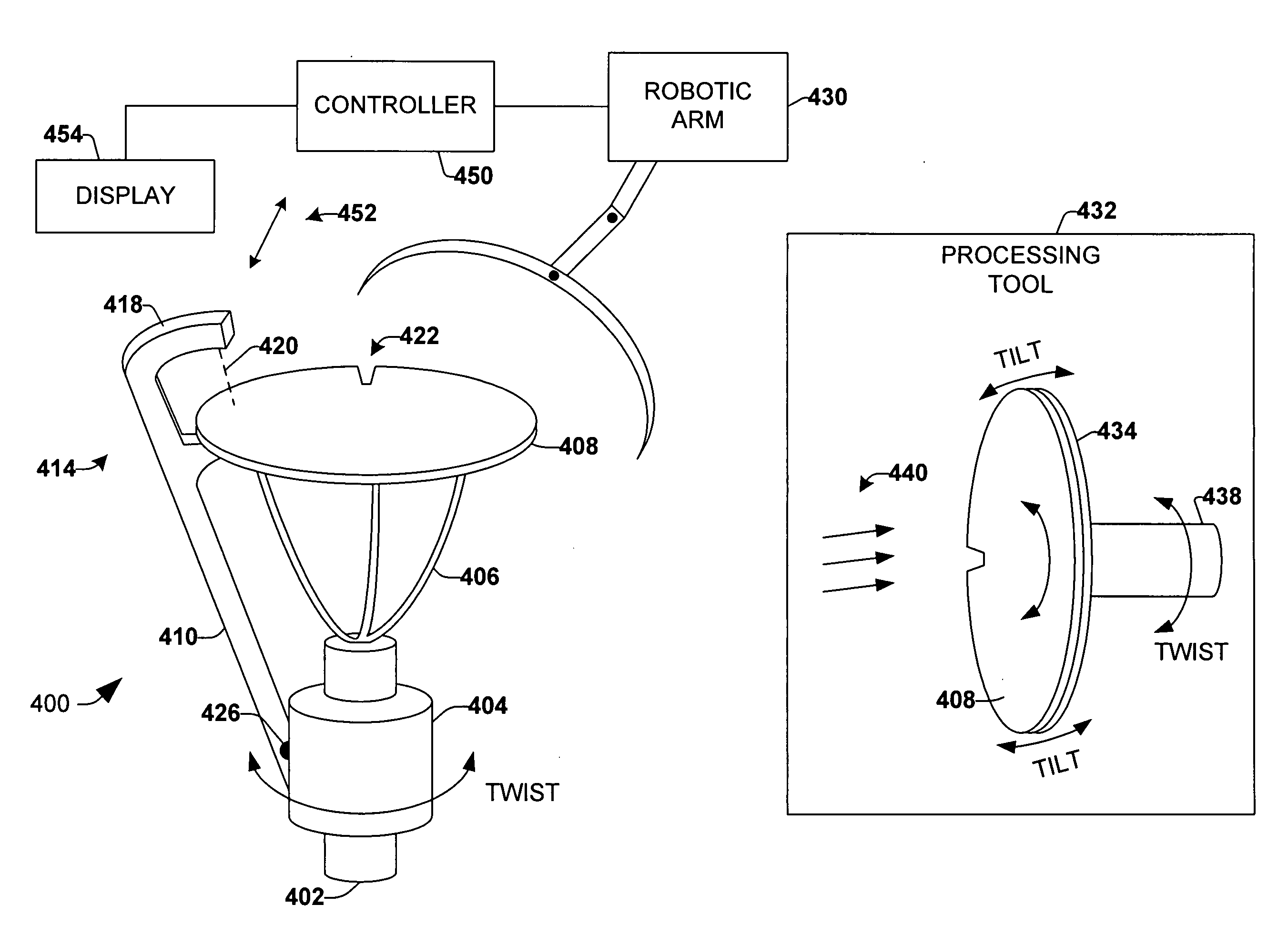
[0025] The present invention is directed to aligning wafers within semiconductor fabrication tools. More particularly, one or more aspects of the present invention pertain to quickly and efficiently finding ...


PUM


Abstract

The present invention is directed to aligning wafers within semiconductor fabrication tools. More particularly, one or more aspects of the present invention pertain to quickly and efficiently finding an alignment marking, such as an alignment notch, on a wafer to allow the wafer to be appropriately oriented within an alignment tool. Unlike conventional systems, the notch is located without firmly holding and spinning or rotating the wafer. Exposure to considerable backside contaminants is thereby mitigated and the complexity and / or cost associated with aligning the wafer is thereby reduced.

Description

FIELD OF THE INVENTION [0001] The present invention relates generally to semiconductor fabrication, and more particularly to a technique for simplifying wafer alignment. BACKGROUND OF THE INVENTION [0002] Wafers used in semiconductor fabrication are typically formed from a crystalline material, such as bulk silicon. In particular, very specific types of single crystals of silicon, known as boules, are grown into long lengths and thin slices (e.g., wafers) are cut there-from. The crystalline structure of the wafers is advantageous in forming semiconductor devices because it facilitates control over the electrical properties of the devices and exhibits uniform electrical performance throughout the entire semiconductor material. Additionally, because impurities that degrade device performance tend to collect around irregularities in the atomic structure of a material, the regularity of the crystalline structure provides for very predictable device performance and yield. [0003] In formi...

Claims


Application Information

Patent Timeline
Patent Type & Authority Applications(United States)
IPC IPC(8): H01L21/00
CPCY10S414/135H01L21/67259H01L2223/54426
Inventor RAY, ANDREW M.
Owner AXCELIS TECHNOLOGIES
Why Eureka
Try Eureka