Multi-port memory device having serial I/O interface

a memory device and serial i/o technology, applied in the field of semiconductor memory design technology, can solve the problems of increasing the cost of transmission, difficulty in packaging, and slow serial transmission method

Active Publication Date: 2005-11-10
SILICON IMAGE INC
View PDF6 Cites 60 Cited by
  • Summary
  • Abstract
  • Description
  • Claims
  • Application Information

AI Technical Summary

Benefits of technology

[0056] It is, therefore, an object of the present invention to provide a multi-port memory device having a serial I/O interface, which is c

Problems solved by technology

However, in recent years, a function separation between the memory device and the chipset has been ambiguous and an integration of the chipset and the memory device has been considered.
Therefore, if a distance is long, a transmission cost increases.
However, compared with the parallel transmission method, the serial transmission method is not

Method used


Image

  • Multi-port memory device having serial I/O interface
  • Multi-port memory device having serial I/O interface
  • Multi-port memory device having serial I/O interface

Examples


Embodiment Construction

[0077] Hereinafter, the present invention will be described in detail with reference to the accompanying drawings.

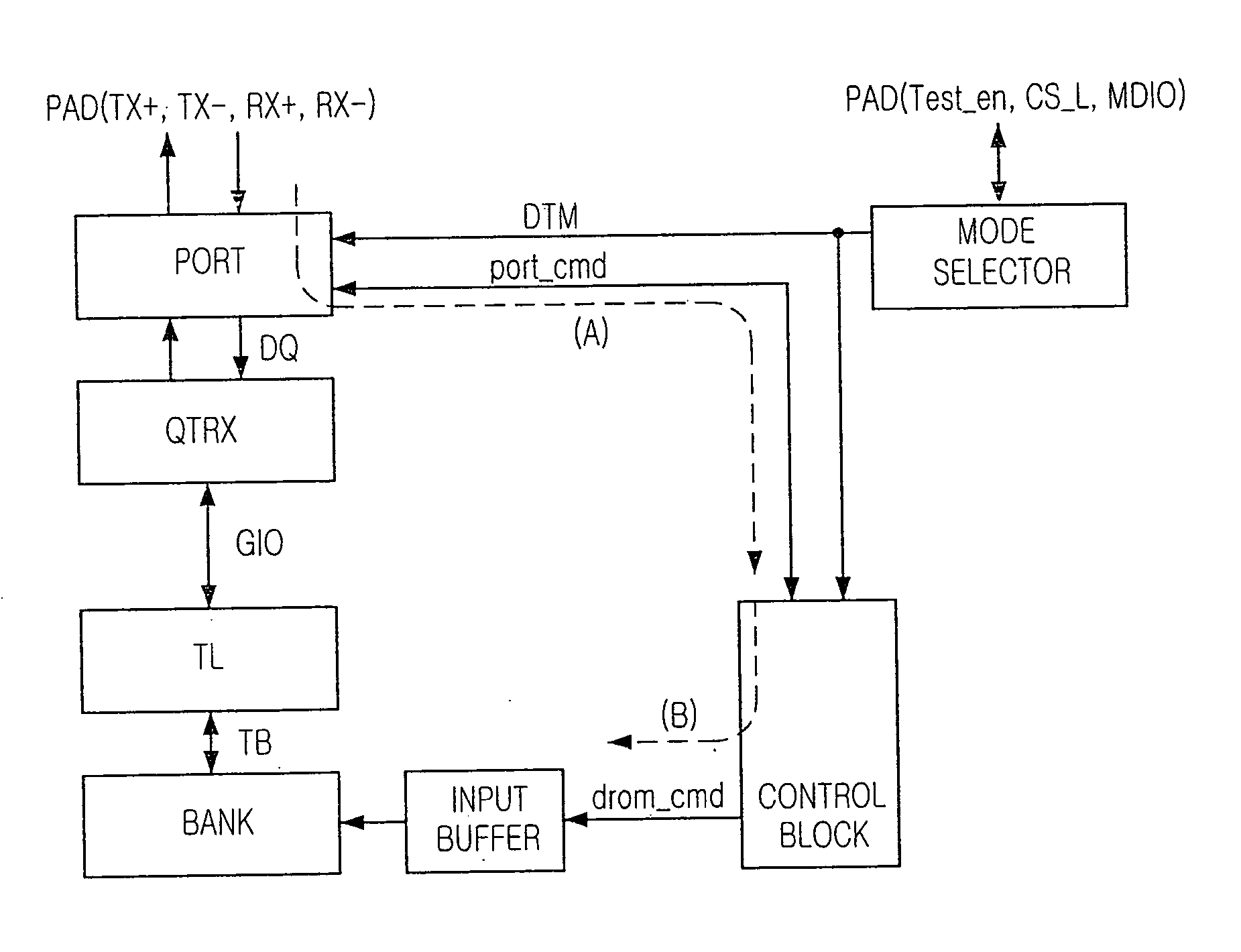
[0078]FIG. 7 illustrates all signals provided to a memory core of a 256M multi-port DRAM shown in FIG. 1.

[0079] Referring to FIG. 7, 64-bit data mask signals DMm and 512-bit write data WDATAm are provided from a port buffer to a memory core.

[0080] A control block generates internal command signals, internal address signals, and control signals, control signals, and an internal clock iCLK. Here, the internal command signals include an internal activation command signal ACT, an internal inactivation command signal PCG, an internal read command signal RD, an internal write command signal WD, and so on. The internal address signals include an activation array address AAA, an inactivation array address PAA, a read array address RAA, a write array address WAA, a row address RA, a read segment address RSA, a write segment address WSA, and so on. The control signals include a...


PUM


Abstract

There is provided a multi-port memory device having a serial I/O interface, which is capable of providing an operation test without any collision with an internal command/address generation path through a limited external pin. The multi-port memory device includes a plurality of ports supporting a serial I/O interface, and the plurality of ports includes a transmission pad and a reception pad. The multi-port memory device includes: a memory core; a control block for generating an internal command signal, an internal address and a control signal, which correspond to the command and are necessary for an operation of the memory core, using commands and addresses inputted to the plurality of ports in a packet form; and a mode selection block for combining signals applied to a plurality of mode selection pads and generating a test mode flag signal, in which I/O data assigned to the transmission pad and the reception pad in a test mode in response to the test mode flag signal are exchanged with the memory core through the ports. Also, the command, the address and the control signal assigned to the transmission pad and the reception pad in the test mode are bypassed at the control block and provided to the memory core.

Description

FIELD OF THE INVENTION [0001] The present invention relates to a semiconductor memory design technology; and, more particularly, to a test related technology of a multi-port memory device having a serial I / O interface. DESCRIPTION OF RELATED ART [0002] Most of memory devices, including a random access memory (RAM), have one port. Also, one port has a plurality of input / output pin sets. In other words, the memory device has only one port for data exchange with chipset. However, in recent years, a function separation between the memory device and the chipset has been ambiguous and an integration of the chipset and the memory device has been considered. This tendency demands a multi-port memory device that can directly exchange data with peripheral graphic devices, CUP, and so on. In order to implement such a multi-port memory device, any one of a plurality of ports must be able to provide an access to all memory cells. [0003] Most of memory devices including RAM use parallel I / O inter...

Claims


Application Information

Patent Timeline
IPC IPC(8): G11C5/02G11C7/10G01R31/28G11C8/16G11C11/401G11C11/4063G11C29/00G11C29/04G11C29/26
CPCG11C29/26G11C8/16G11C7/1075G11C2207/105
Inventor LEE, IHL-HO
Owner SILICON IMAGE INC
Why Eureka
Try Eureka