Display apparatus, its display module and display panel

Inactive Publication Date: 2005-11-24
HITACHI LTD
View PDF6 Cites 0 Cited by
  • Summary
  • Abstract
  • Description
  • Claims
  • Application Information

AI Technical Summary

Benefits of technology

[0029] According to the present invention, by suppressing deformation of the cathode substrate by use of the pressure support, the displ

Problems solved by technology

In this point, a problem about the lightening remains.
However, a flexural rigidity of the anode substrate is not improved so much.
According

Method used


Image

  • Display apparatus, its display module and display panel
  • Display apparatus, its display module and display panel
  • Display apparatus, its display module and display panel

Examples


Example

[0045] A display apparatus of a first embodiment of the present invention is explained with reference to FIGS. 1 to 13.

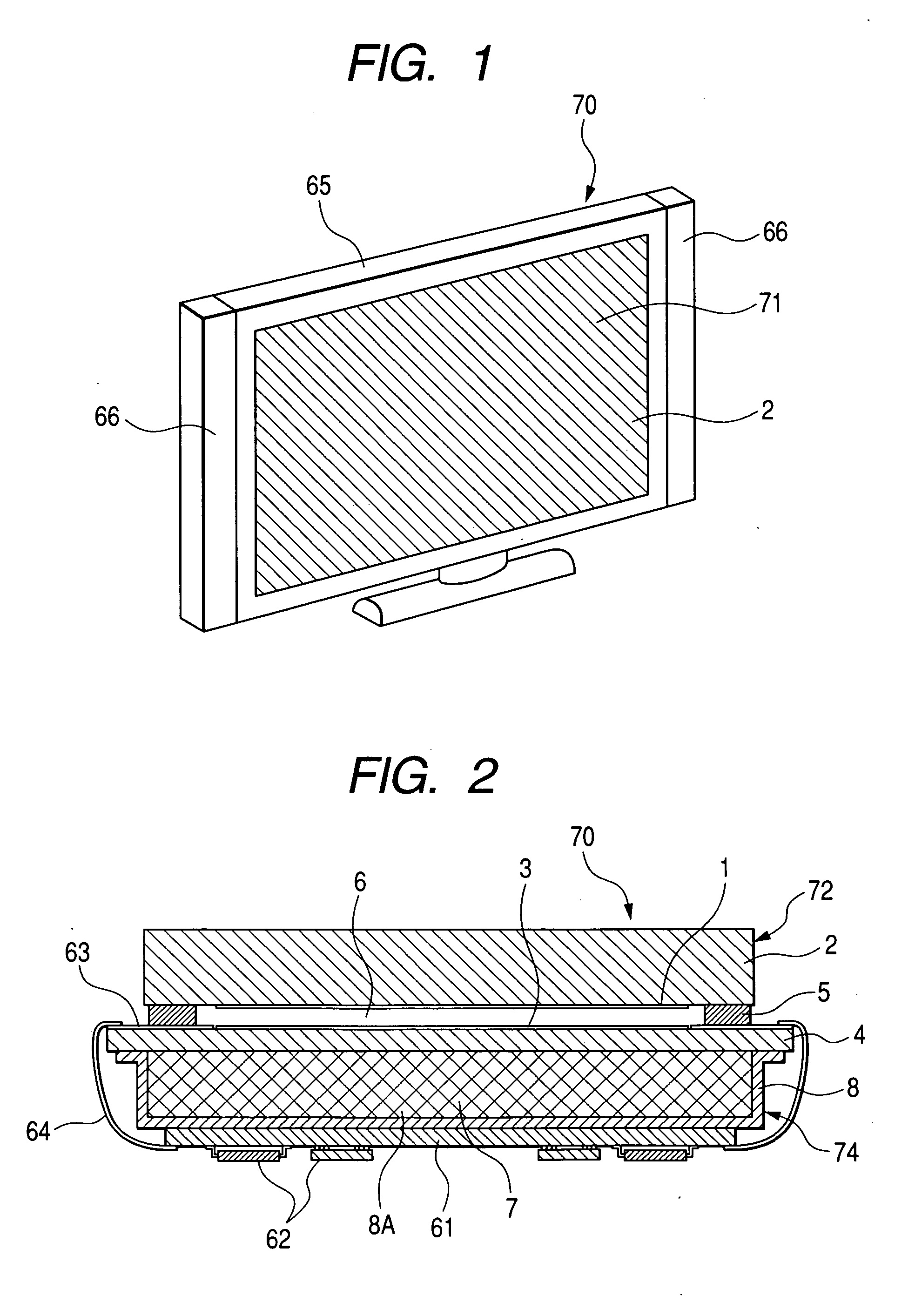
[0046] First, an overall structure of a display apparatus 70 of this embodiment is explained with reference to FIG. 1. FIG. 1 is an external perspective view of the display apparatus 70 of this embodiment.

[0047] This display apparatus 70 is an example applied to a television set, and includes a body 65, a display panel module 71, and speakers 66. The display apparatus of the present invention is applicable to a display apparatus for, e.g., a personal computer and DVD.

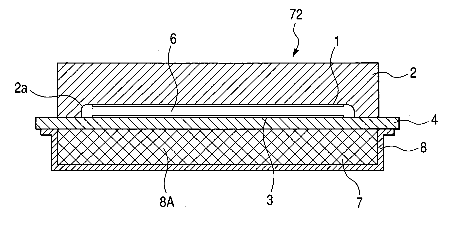
[0048] A display panel module 71 is thin and light, and mounted in the body 65. An anode substrate 2 of the display panel module 71 is exposed from a front window (shaded portion of FIG. 1) of the body 65 in a planar fashion. In this embodiment, the display panel module 71 is applicable to a panel having a screen over thirty-two inches. A transparent protection film is applied to a surface of the ano...

Example

[0086] Next, a second embodiment of the present invention is explained with reference to FIGS. 13 and 14. FIG. 13 is a cross sectional view of the display panel 72 in the display apparatus of the second embodiment of the present invention. FIG. 14 is a perspective view of the display panel 72 which is partially cut. This second embodiment is different from the first embodiment in the after-mentioned points. In the other points, the second embodiment is basically the same as the first embodiment.

[0087] In this second embodiment, a small number of spacers 52 are placed between the anode substrate 2 and cathode substrate 4. Since the spacers 52 support the anode substrate 2 when the anode substrate 2 is pressed toward the inside of the electron emitting chamber 6 due to the atmospheric pressure, the anode substrate 2 flexes small even when the anode substrate 2 is thinned, and an appropriate space can be maintained between the phosphors 1 and electron sources 3. As a result, the anode...


PUM


Abstract

To achieve high resolution, lightening, and thinning in a display apparatus, the display apparatus includes a thin display panel and a control unit. The display panel includes an anode substrate, a cathode substrate forming an electron emitting chamber vacuously sealed between itself and the anode substrate, phosphors formed on the anode substrate, and a pressure support formed on the back of the electron emitting chamber side of the cathode substrate. The pressure support includes a vacuum seal member forming a pressure supporting chamber vacuously sealed between itself and the cathode substrate independently of the electron emitting chamber, and a reinforcement member which is formed of a member having a gap, which is sandwiched between the vacuum seal member and cathode substrate in the pressure supporting member, and at least both end portions of which span a bonding area of the cathode substrate for the anode substrate.

Description

CLAIM OF PRIORITY [0001] The present application claims priority from Japanese application serial JP 2004-151334 filed on May 21, 2004, the content of which is hereby incorporated by reference into this application. FIELD OF THE INVENTION [0002] The present invention relates to a display apparatus, its display module and display panel. Particularly, the present invention is appropriate for a field emission display apparatus. BACKGROUND OF THE INVENTION [0003] A basic structure of a field emission display apparatus is described in, for example, the special feature “Basic knowledge of an electronic display for young engineers” in the April 2004 issue of a technical magazine “Electronic Material”, pages 94 to 102 (non-patent document 1). The field emission display apparatus is so structured that a cathode substrate on which many electron sources for emitting electrons are formed and an anode substrate to which phosphors are applied are placed opposite each other via a gap. Electrons em...

Claims


Application Information

Patent Timeline
IPC IPC(8): H01J29/86G09F9/00G09F9/30G09F9/313H01J1/62H01J29/87H01J31/12H01J63/04
CPCH01J31/123H01J29/87
Inventor KAZAMA, ATSUSHITERASAKI, TAKESHIKITANO, MAKOTONAGATA, TATSUYAFUJIMURA, TAKASHI
Owner HITACHI LTD
Why Eureka
Try Eureka