Method for fabricating leadless packages with mold locking characteristics

a technology of mold locking and leadless semiconductors, applied in semiconductor devices, semiconductor/solid-state device details, electrical devices, etc., can solve the problems of inability to enhance the horizontal mold locking of the die pad b>11, against the package body, etc., to achieve easy delaminate, avoid defeat, and easy filling of the package body

Active Publication Date: 2005-11-24
ADVANCED SEMICON ENG INC
View PDF3 Cites 32 Cited by
  • Summary
  • Abstract
  • Description
  • Claims
  • Application Information

AI Technical Summary

Benefits of technology

[0024] Referring to FIG. 7, when the leadless leadframe 100 mentioned above is implemented in manufacturing a semiconductor package, a semiconductor package comprises the die pad 110 and the leads 120 from the leadless leadframe 100. A semiconductor chip 210 is attached to the upper surface 111 of the die pad 110. A plurality of bonding wires 220 connect the bonding pads 211 of the semiconductor chip 210 to the upper surfaces 121 of the leads 120. At least one of the bonding wires 220 connects the ground pad of the chip 210 to the peripheral portion of the upper surface 111 of the die pad 110 or the tie bar 115 which is plated with the metal layer 130. A package body 230 including electrically insulated resin is formed on the leadless leadframe 100. The package body 230 encapsulates the semiconductor chip 210 and the bonding wires 220, and fills the indentations 114 of the die pad 110 and the mold locking blind holes 123 of the leads 120. As shown in FIG. 8, the lower surface 112 of the die pad 110 and the lower surface 122 of the leads 120 are exposed out of the bottom of the package body 230 for heat dissipation and electrical connection to the outside world. When the semiconductor package mentioned above passes through a thermal test, the indentations 114 can disperse the horizontal thermal stress and firmly hold the sidewall 113 of the die pad 110 with the package body 230 in the horizontal direction. Therefore, the sidewall 113 of the die pad 110 will not easily delaminate from the package body 230. Moreover, the mold locking blind holes 123 are able to hold the leads 120 in the horizontal direction firmly to avoid any defeats during singulation. Although, in the first embodiment, the chip 210 is electrically connected to the leads 120 through the bonding wires 220. But the leadless leadframe 100 not only can be used for packaging a wire-bonding chip, also can be used for packaging a flip chip. Referring to FIG. 9, a flip chip 240 can be flip-chip mounted to the leadless leadframe 100 in the second embodiment. A plurality of bumps 241 are attached onto the flip chip 240 and are connected to the leads 120. Moreover, the flip chip 240 is attached to the die pad 110 using at least a dummy bump 242, and ground bumps, adhesive tapes or liquid compounds can be an alternative to fix the flip chip 240 on the die pad 110. In accordance with the third embodiment of the present invention a leadless leadframe with an improved die pad for mold locking is shown in FIGS. 10, 11 and 12. The leadless leadframe 300 in each packaging unit comprises a die pad 310 and a plurality of leads 320. The die pad 310 has an upper surface 311, a lower surface 312 and at least a sidewall 313. The leads 320 are arranged around the die pad 310. A plurality of indentations 314 are formed in the sidewall 313 of the die pad 310. The indentations 314 are vertical grooves extending from the periphery of the upper surface 311. In this embodiment, the indentations 314 are V-shaped, U-shaped or semicircle shaped grooves on the periphery of the upper surface 311 as shown in FIGS. 10 and 11. As shown in FIG. 12, a half-etching portion 315 is formed at the periphery of the lower surface 312 of the die pad 310 and the periphery of the lower surface of the leads 320, so that the area of the upper surface 311 is larger than the area of the lower surface 312. Thus the indentations 314 may not extend to the lower surface 312 of the die pad 310. Moreover, the die pad 310 has at least a mold locking through hole 316 which is formed in the upper surface 311 of the die pad 310 corresponding to the half-etching portion 315. The mold locking through hole 316 does not extend to the lower surface 312 of the die pad 310 for easily filling a package body. Therefore, the horizontal mold locking capability of the die pad 310 can be enhanced by means of the indentations 314. In a semiconductor package, a package body can fill the indentations 314 so that the die pad 310 will not easily delaminate from the package body in the horizontal direction. Moreover, each lead 320 has a necking portion 317 to connect to the frame of the leadless leadframe 300 for singulation.
[0025] In accordance with the fourth embodiment of the present invention another leadless leadframe 400 with an improved die pad for mold locking is shown in FIG. 13. The components disclosed in the fourth embodiment are almost the same as those in the third embodiment. The leadless leadframe 400 comprises a die pad 410 and a plurality of leads 420. The leads 420 are arranged around the die pad 410. A plurality of indentations 411 are formed in the sidewall 414 for enhancing the horizontal mold locking capability of the die pad 410 in the leadless semiconductor package. A mold locking through hole 413 is formed in the die pad 410 corresponding to the half-etching portion 412. In this embodiment, the edge between the upper surface of the die pad 410 and the sidewall 414 are oblique. Preferably, the leads 420 includes an lead 421 that is connected to the die pad 410 for changing the position of the ground terminal of the die pad 410.
[0026] In addition, a method for fabricating leadless semiconductor packages using the leadframe 100 is also disclosed. Firstly, please refer to FIGS. 14A and 3, the leadframe 100 with the improved die pads 110 is provided. The units 101 of the leadframe 100 are arranged in a matrix. Connecting bars 102 are formed between the units 101. Each die pad 110 is formed inside the corresponding unit 101 and is surrounded by the leads 120. Then, referring to FIG. 14B, a plurality of chip 210 are attached to the upper surfaces 111 of the die pads 110 by means of adhesive compounds, tapes, eutectic layers or bumps, etc. Each chip 210 has a plurality of bonding pads 211 on the active surface thereof. Preferably, a step of electrically connection is performed. As shown in FIG. 14C, a plurality of bonding wires 220 are formed by a wire bonder to connect the bonding pads 211 of the chips 210 to the leads 120. Then, referring to FIG. 14D, a plurality of package bodies 230 are formed on the units 101. In this embodiment, the package bodies 230 are formed by molding using a mold tool with a plurality of mold cavities (not shown in figures), so that the package bodies 230 on the leadframe 100 are individually separated and connected to each other via the connecting bars 102. The package bodies 230 cover the active surfaces of the chips 210, the bonding wires 220 and the upper surfaces 121 of the leads 120 in the corresponding units 101. Also the indentations 114 of the die pads 110 and the mold locking blind vias 123 are filled with the package bodies 230. But the lower surfaces 122 of the leads 120 and the lower surfaces 112 of the die pads 110 are exposed out of the corresponding package bodies 230. However, the connecting bars 102 are free from the package bodies 230 on their upper surfaces. Then as shown in FIG. 14E, a punching step is performed. The connecting bars 102 are punched out to efficiently isolate a plurality of individual leadless packages from the leadframe. Therefore, singulation efficiency of the leadless packages in a matrix is improved to increase throughput.

Problems solved by technology

However, the reentrant portion 13 is annular design in the horizontal direction, therefore, it's unable to enhance the horizontal mold locking of the die pad 11 against the package body 40.

Method used


Image

  • Method for fabricating leadless packages with mold locking characteristics
  • Method for fabricating leadless packages with mold locking characteristics
  • Method for fabricating leadless packages with mold locking characteristics

Examples


Embodiment Construction

[0021] Please refer to the drawings attached, the present invention will be described by means of an embodiment below.

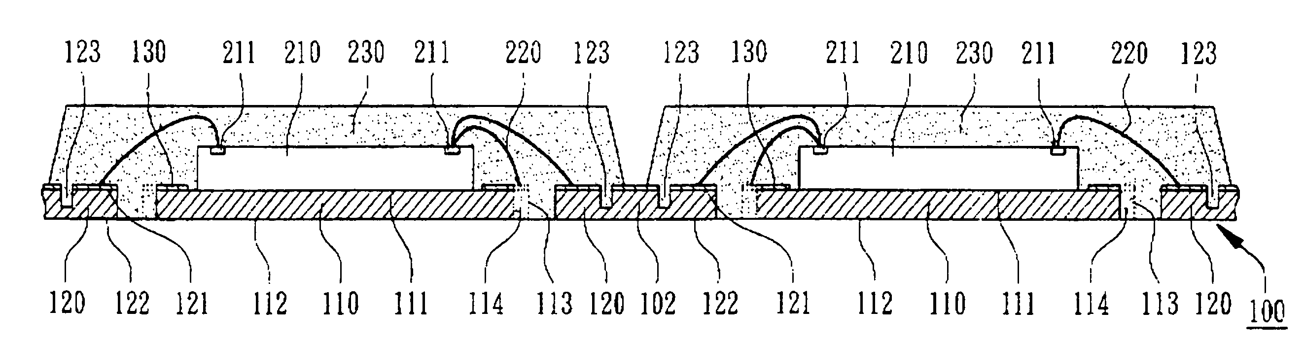
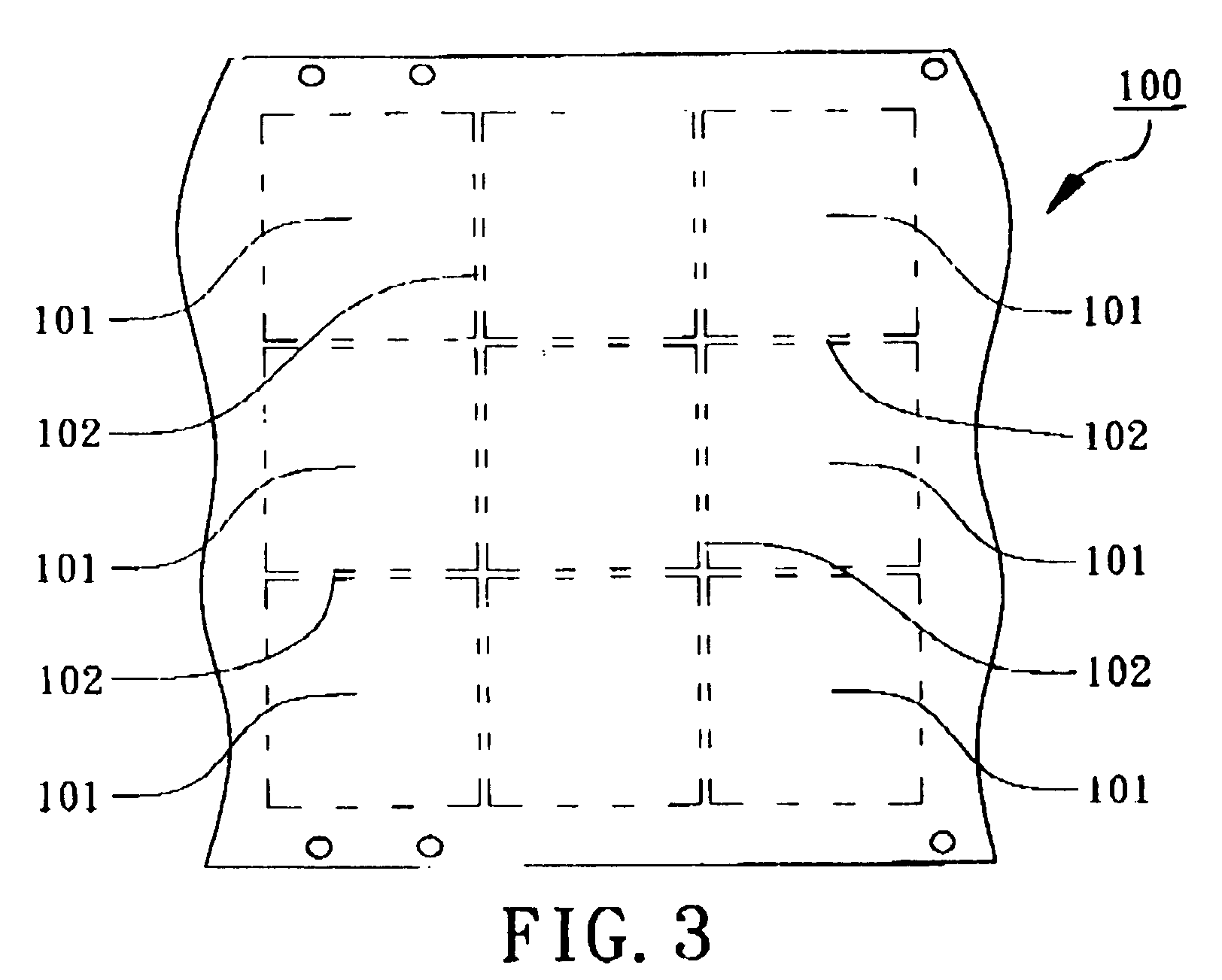
[0022] According to the first embodiment of the present invention, a leadless leadframe 100 with an improved die pad for mold locking is shown in FIGS. 3, 4, 5, and 6. As shown in FIG. 3, the leadframe 100 has a plurality of units 11 in a matrix and a plurality of connecting bars 102 between the units 101. As shown in FIG. 4, the leadframe 100 in each unit 101 comprises a die pad 110 and a plurality of leads 120, which are connected together via the connecting bars 102. As shown in FIG. 6, the die pad 110 has an upper surface 111, a lower surface 112 and at least a sidewall 113. The sidewall 113 is located between the upper surface 111 and the lower surface 112. The sidewall 113 can be vertical or oblique. The height of the sidewall 113 can be equal to or smaller than the thickness of the die pad 110. As shown in FIG. 7, the upper surface 111 of the die pad 110 is c...


PUM


Abstract

A method for fabricating leadless packages with mold locking characteristics is disclosed. A provided leadless leadframe has a plurality of units in a matrix, each unit includes an improved die pad with a plurality of indentations, such as semi-vias in the sidewall thereof and a plurality of leads around the die pad. After chip attachment and electrical connection, a plurality of package bodies for semiconductor packages are individually formed on the corresponding units and covered the indentations in order to enhance the horizontal mold locking capability of the die pad. Using punching, connecting bars of the leadless leadframe are removed to isolate the leadless packages.

Description

FIELD OF THE INVENTION [0001] The present invention relates to a method for fabricating leadless semiconductor packages, and more particularly, to a method for fabricating leadless semiconductor packages using a leadframe with improved die pads. BACKGROUND OF THE INVENTION [0002] A leadless leadframe can be implemented in semiconductor package with lower costs and smaller dimensions. A well-know leadless semiconductor package comprises a semiconductor chip, a leadless metal leadframe for carrying a chip and a package body for encapsulating the chip. A plurality of leads of the leadless leadframe have the lower surfaces exposed out of the bottom of the package body for external mounting onto an PCB. Normally, no outer leads extending from sides of the package body are needed. The leadless semiconductor package has the benefits of smaller footprints, shorter electrical paths, and lower manufacturing costs. [0003] A leadless semiconductor package is disclosed in U.S. Pat. No. 6,143,981...

Claims


Application Information

Patent Timeline
Patent Type & Authority Applications(United States)
IPC IPC(8): H01L21/58H01L23/31H01L23/495
CPCH01L23/3107H01L2224/0401H01L23/49568H01L23/49582H01L24/15H01L24/48H01L24/97H01L2224/05599H01L2224/05639H01L2224/05644H01L2224/05655H01L2224/13099H01L2224/16245H01L2224/48091H01L2224/48247H01L2224/48257H01L2224/484H01L2224/85399H01L2224/85439H01L2224/85444H01L2924/01006H01L2924/01028H01L2924/01047H01L2924/01079H01L2924/01082H01L2924/01322H01L2924/18301H01L23/49503H01L2924/01033H01L2924/01023H01L2924/00014H01L2224/45099H01L2924/181H01L2924/351H01L2924/00H01L2924/00012
Inventor PARK, SANG-BAELEE, YONG-GILLPARK, HYUNG-JUNRHO, KYUNG-SOOWON, JIN-HEE
Owner ADVANCED SEMICON ENG INC
Why Eureka
Try Eureka