

Semiconductor devices having phase change memory cells, electronic systems employing the same and methods of fabricating the same
- Summary
- Abstract
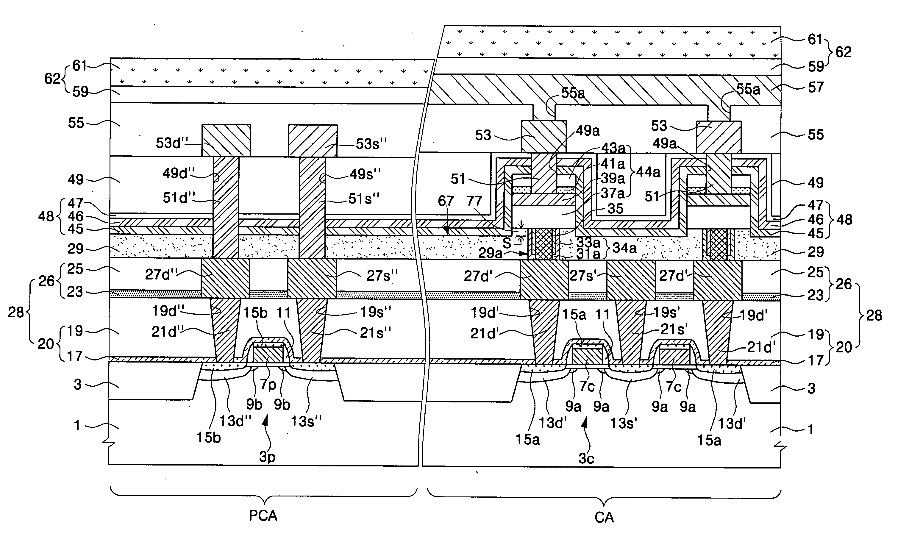
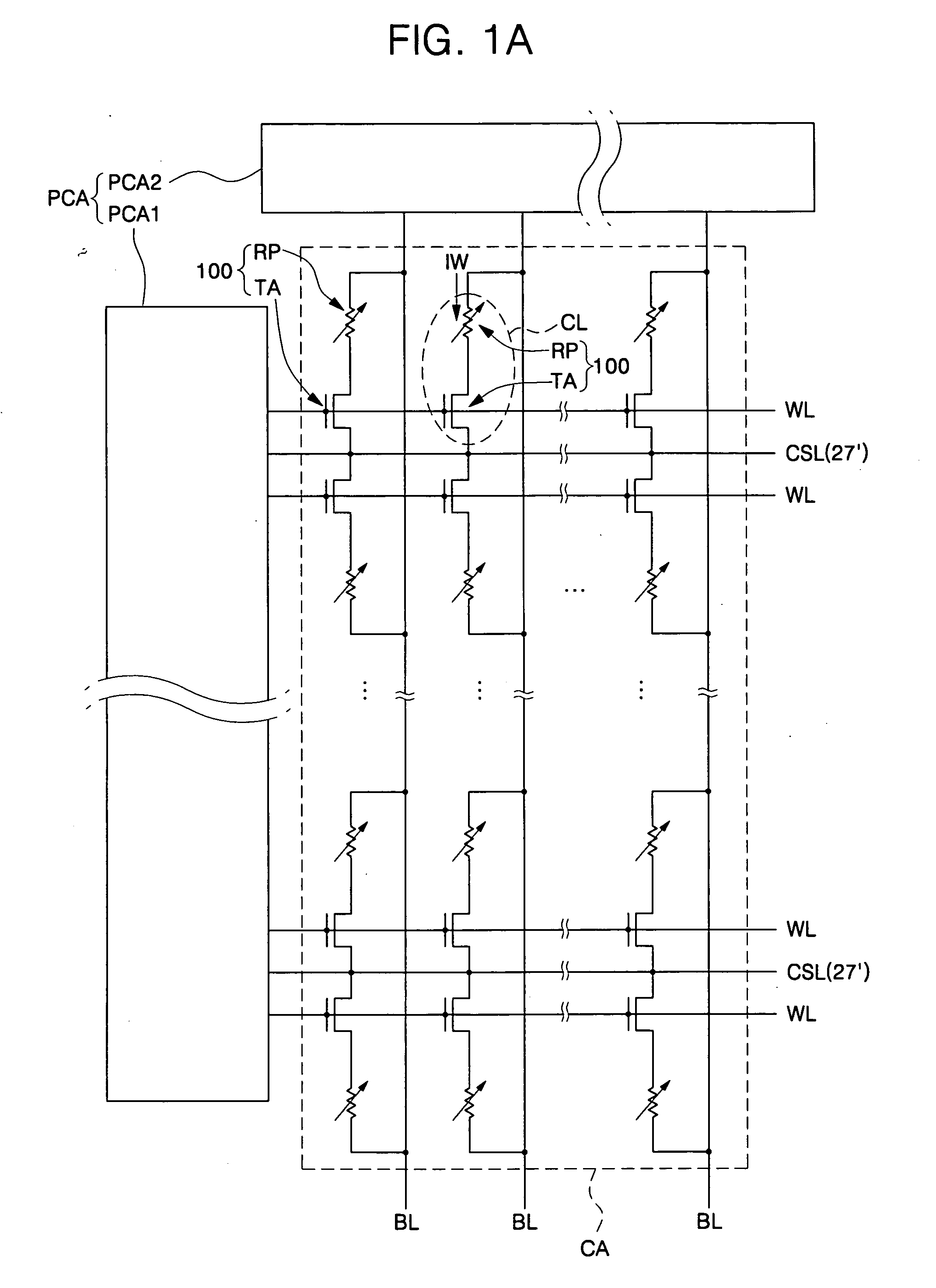
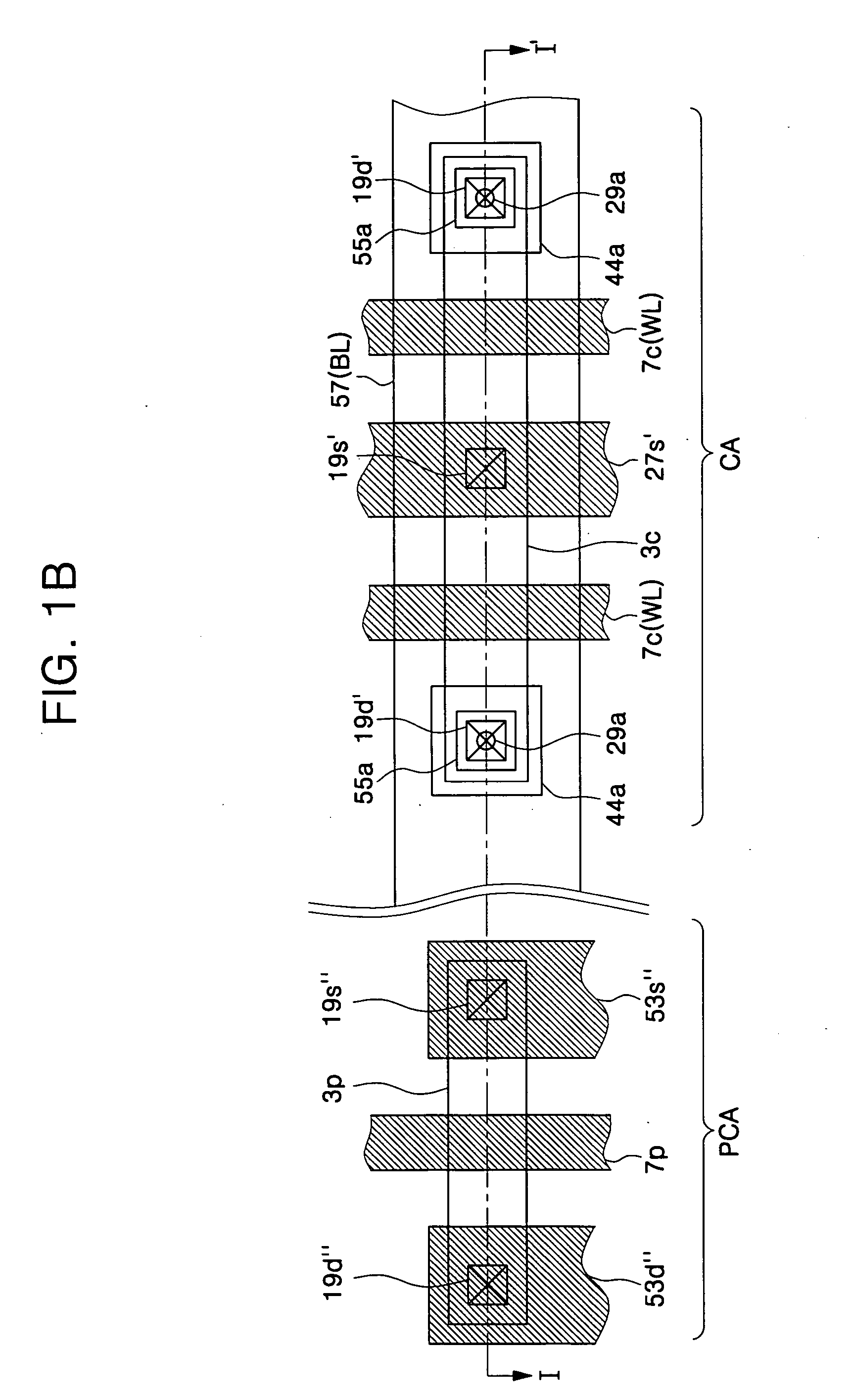
- Description
- Claims
- Application Information
AI Technical Summary
Benefits of technology
Problems solved by technology
Method used
Image

Examples
examples
[0072]FIG. 17 is a graph illustrating set / reset resistance characteristics of the phase-change memory cells fabricated according to the present invention and the conventional art. In FIG. 17, a horizontal axis represents a diameter D of the phase-change material patterns, and a vertical axis represents a resistance R of the phase-change resistors. In the graph of FIG. 17, the data indicated by reference letters “NR” and “NS” represent a reset resistance and a set resistance of the conventional phase-change resistors fabricated without an oxidation barrier layer, respectively. The data indicated by reference letters “SR” and “SS” represent a reset resistance and a set resistance of the phase-change resistors covered with a single oxidation barrier layer, respectively. Further, the data indicated by reference letters “DR” and “DS” represent a reset resistance and a set resistance of the phase-change resistors covered with a double oxidation barrier layer, respectively. The phase-chang...
PUM
 Abstract
Description
Claims
Application Information