Structure for inverted F plane antenna

a technology of antenna structure, which is applied in the direction of antennas, elongated active element feeds, basic electric elements, etc., can solve the problems of narrow operation bandwidth of the inverted f plane antenna set forth above, and achieve the effect of increasing the total length of the antenna, improving signal receiving and emission quality, and increasing operation bandwidth

Inactive Publication Date: 2005-12-01
CHUNG GUAN TECH
View PDF1 Cites 16 Cited by
  • Summary
  • Abstract
  • Description
  • Claims
  • Application Information

AI Technical Summary

Benefits of technology

[0007] Another object of the invention is to provide an inverted F plane antenna structure with increased operation bandwidth.
[0008] Yet another object of the invention is to provide an inverted F plane antenna structure to improve signal receiving and emission quality.
[0009] In order to achieve the foregoing objects, the inverted F plane antenna structure according to the invention is formed on the surface of a PCB by etching. It has a pair of parallel sections connecting by a vertical section. The first parallel section is electrically connected to a grounding end of the PCB, while the second parallel section is electrically connected to a signal end of the PCB. The vertical section has at least one bending section formed in U-shape to increase the total length of the antenna. Thereby reflection signals may be reduced and signals of a greater power range may be received and emitted. And the receiving and emission bandwidth increases. In addition, the antenna size may be shrunk to facilitate antenna design without increasing the length of the vertical section.

Problems solved by technology

However, the conventional inverted F plane antenna set forth above usually has a narrow operation bandwidth.

Method used


Image

  • Structure for inverted F plane antenna
  • Structure for inverted F plane antenna
  • Structure for inverted F plane antenna

Examples


Embodiment Construction

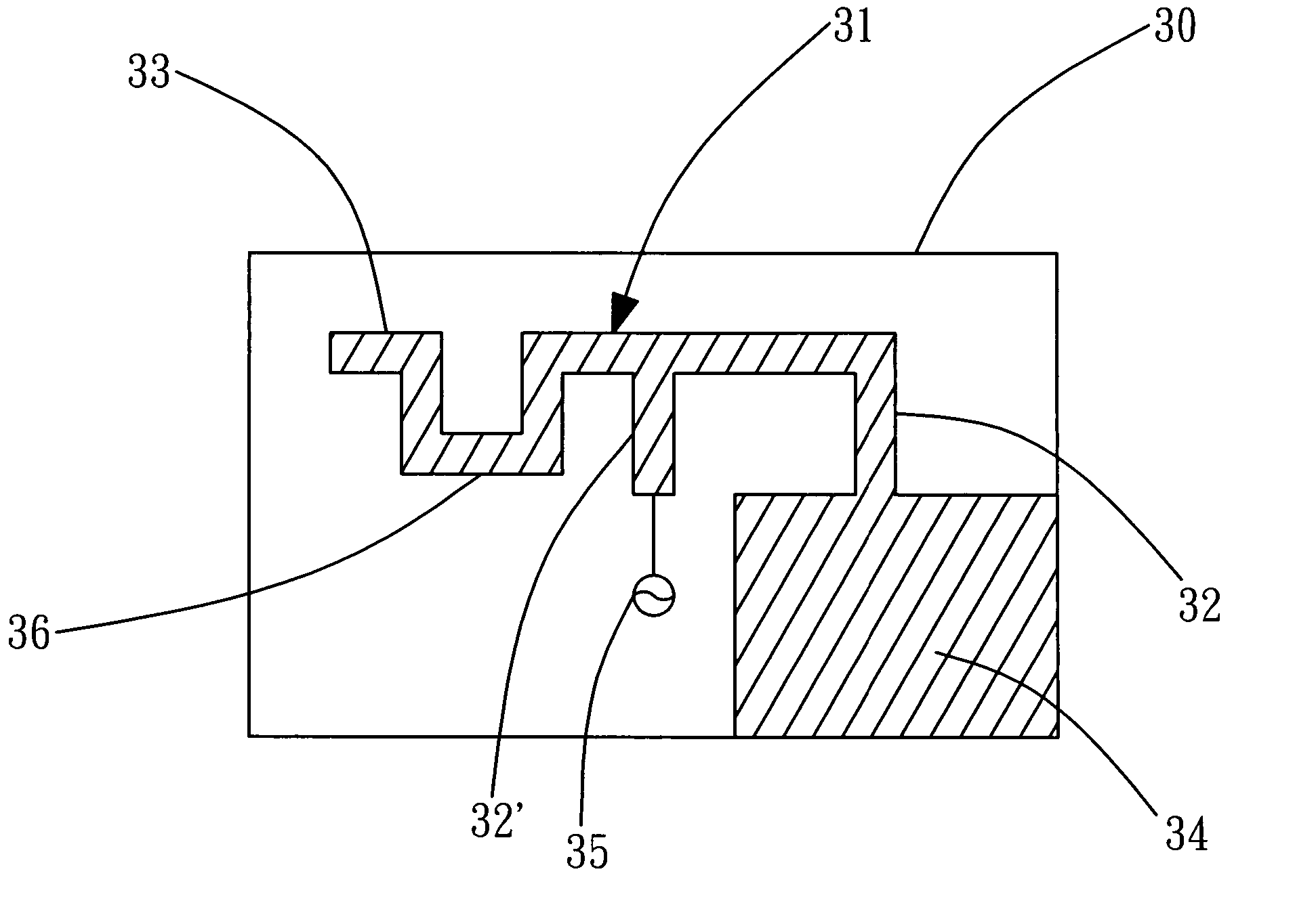
[0015] Referring to FIG. 3, the inverted F plane antenna structure according to the invention includes an inverted F plane antenna 31 formed on a surface of a PCB 30 by etching. The antenna 31 has a pair of parallel sections that include a first parallel section 32 and a second parallel section 32′ and a vertical section 33 connecting to the first parallel section 32 and the second parallel section 32′ in a perpendicular manner. The first parallel section 32 is electrically connected to a grounding end 34 of the PCB 30, while the second parallel section 32′ is electrically connected to a signal end 35 of the PCB 30. The vertical section 33 has at least one bending section 36 formed in U-shape to increase the total length of the antenna 31.

[0016] Because the total length of the antenna 31 increases, it can receive and emit signals of a lower frequency and a greater power range, and also increase the receiving and emission bandwidth. Therefore, the antenna size may be shrunk without ...


PUM


Abstract

The present invention is related to a structure for inverted F plane antenna, which is on a surface of a PCB by way of etching. The antenna comprises a pair of parallel sections constructed by a first parallel section, a second parallel section and a vertical section perpendicular to the two parallel sections, wherein the first parallel section connects to a grounding end of the PCB electrically, the second parallel section connects to a power end of the PCB, the vertical section has a bending portion with U shape to increase the length of receiving signals, therefore reflection signals may be highly decreased, and functions of receiving/emission stronger power are then achieved and receiving/emission band width is increased; further, under conditions of not extending the length of the vertical section and shrinking the volume of the antenna shall upgrade the convenience of the design.

Description

FIELD OF THE INVENTION [0001] The present invention relates to a structure of an inverted F plane antenna and particularly to an inverted F plane antenna that has a greater operation bandwidth and a smaller size. BACKGROUND OF THE INVENTION [0002] With rapid development of wireless communication technologies, 3C (consumption, communication and computer) products that are coupled with communication modules to form mobile communication products have become the main stream of the current technology products, such as notebook computer, PDA and the like. These products, after coupled with the communication module, not only can be connected to a local area network (LAN) to receive and transmit e-mail, also can receive instant information (such as instant news, stock quotations, etc.) to achieve resources sharing and data transmission functions. Inverted F plane antenna is small and light, thus is widely used as a built-in antenna of the mobile communication products.. [0003] Refer to FIG....

Claims


Application Information

Patent Timeline
Patent Type & Authority Applications(United States)
IPC IPC(8): H01Q1/38H01Q9/04
CPCH01Q1/38H01Q9/0421H01Q9/42
Inventor SHAN, CHI-SHEN
Owner CHUNG GUAN TECH
Why Eureka
Try Eureka